
Page 176 - Organic Electronics in Sensors and Biotechnology
P. 176
Integrated Pyr oelectric Sensors 153
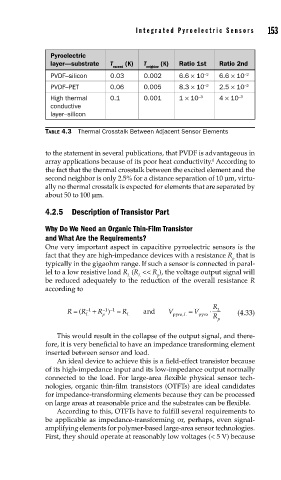
Pyroelectric
layer—substrate T (K) T (K) Ratio 1st Ratio 2nd
exceed neighbor
PVDF–silicon 0.03 0.002 6.6 × 10 –2 6.6 × 10 –2
PVDF–PET 0.06 0.005 8.3 × 10 –2 2.5 × 10 –2
High thermal 0.1 0.001 1 × 10 –3 4 × 10 –3
conductive
layer–silicon
TABLE 4.3 Thermal Crosstalk Between Adjacent Sensor Elements
to the statement in several publications, that PVDF is advantageous in
6
array applications because of its poor heat conductivity. According to
the fact that the thermal crosstalk between the excited element and the
second neighbor is only 2.5% for a distance separation of 10 μm, virtu-
ally no thermal crosstalk is expected for elements that are separated by
about 50 to 100 μm.
4.2.5 Description of Transistor Part
Why Do We Need an Organic Thin-Film Transistor
and What Are the Requirements?
One very important aspect in capacitive pyroelectric sensors is the
fact that they are high-impedance devices with a resistance R that is
p
typically in the gigaohm range. If such a sensor is connected in paral-
lel to a low resistive load R (R << R ), the voltage output signal will
L L p
be reduced adequately to the reduction of the overall resistance R
according to
R L
−1
−1
R = ( R + R ) −1 ≈ R and V = V ⋅ (4.33)
L p L pyro, L pyro R
p
This would result in the collapse of the output signal, and there-
fore, it is very beneficial to have an impedance transforming element
inserted between sensor and load.
An ideal device to achieve this is a field-effect transistor because
of its high-impedance input and its low-impedance output normally
connected to the load. For large-area flexible physical sensor tech-
nologies, organic thin-film transistors (OTFTs) are ideal candidates
for impedance-transforming elements because they can be processed
on large areas at reasonable price and the substrates can be flexible.
According to this, OTFTs have to fulfill several requirements to
be applicable as impedance-transforming or, perhaps, even signal-
amplifying elements for polymer-based large-area sensor technologies.
First, they should operate at reasonably low voltages (< 5 V) because