
Page 178 - Organic Electronics in Sensors and Biotechnology
P. 178
Integrated Pyr oelectric Sensors 155
form a smooth and dense nanocomposite gate dielectric. Pentacene is
35
used as the organic semiconductor material, the gate electrode is based on
Al, while Au source and drain electrodes are employed. For the substrate
glass or PET film, Melinex is used. The devices are fabricated according
to the following procedure: the gate is formed by thermal evaporation of
aluminum through shadow masks on a glass or PET substrate and the
metal-oxide layer is fabricated by reactive sputtering of Al or Zr under
high vacuum condition. Prior to the active organic semiconductor, a thin
layer (~ 5 to 20 nm) of an appropriate hydroxyl-free polymer (PαMS or
PVCi) was applied to the metal-oxide dielectric layer by spin-coating,
thus forming a dense metal-polymer nanocomposite double layer as
gate dielectric. Finally, for completion of the transistor device, 50 nm of
pentacene is applied by thermal evaporation and structured via shadow
masks at a rate of 0.1 nm/min and a substrate temperature of T = 25°C.
S
According to variable spectroscopic ellipsometry measurements
done on the as-produced nanocomposite gate dielectrics but fabri-
cated on silicon wafers, the measured layer thickness and optical con-
stants can be modeled only if a mixed structure with club-shaped
metal-oxide crystallites and interspaces filled by the polymer is
34
assumed. The club-shaped metal-oxide film growth with interspaces
is clearly seen in the TEM micrograph (Fig. 4.23b). 34
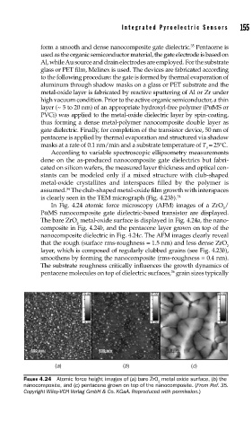
In Fig. 4.24 atomic force microscopy (AFM) images of a ZrO /
2
PαMS nanocomposite gate dielectric-based transistor are displayed.
The bare ZrO metal-oxide surface is displayed in Fig. 4.24a, the nano-
2
composite in Fig. 4.24b, and the pentacene layer grown on top of the
nanocomposite dielectric in Fig. 4.24c. The AFM images clearly reveal
that the rough (surface rms-roughness = 1.5 nm) and less dense ZrO
2
layer, which is composed of regularly clubbed grains (see Fig. 4.23b),
smoothens by forming the nanocomposite (rms-roughness = 0.4 nm).
The substrate roughness critically influences the growth dynamics of
36
pentacene molecules on top of dielectric surfaces, grain sizes typically
15.00 15.00 50.00
0.00 0.00 0.00
400 nm 400 nm 1.0 μm
(a) (b) (c)
FIGURE 4.24 Atomic force height images of (a) bare ZrO metal oxide surface, (b) the
2
nanocomposite, and (c) pentacene grown on top of the nanocomposite. (From Ref. 35.
Copyright Wiley-VCH Verlag GmbH & Co. KGaA. Reproduced with permission.)