
Page 180 - Organic Electronics in Sensors and Biotechnology
P. 180
Integrated Pyr oelectric Sensors 157
I = I (−3 V). The subthreshold swing defined as the inverse of
on ds
the maximum slope of the current in the subthreshold regime is
around S = 100 mV/dec in this device for forward sweep direction.
From the square root dependence of the drain current as a function
of the gate voltage, the threshold voltage V is determined to be
T
about V =−1.3 V (Fig. 4.25), demonstrating that the device can be
T
controlled and operated in the low-voltage regime, similar to penta-
38
cene OTFT devices based on TiO with a PαMS capping layer. It is
2
interesting to mention that in all nanocomposite OTFTs the charge
carrier mobility μ does not depend on the gate field for voltages
2
above V = -2 V, reaching values around μ = 0.4 − 1.2 cm /(V ⋅ s).
gs
The high mobility values nicely correlate with the typical morphol-
ogy of the polycrystalline pentacene layers grown on the nanocom-
posite dielectric surface, where the very large size of the crystallites
is related to a smaller density of transport hindered by grain bound-
aries (Fig. 4.24c). Finally the gate leakage current is below 1 × 10 A,
−9
showing that the prepared transistors reveal a sufficiently high
input impedance (in the GΩ regime) for sensor applications.
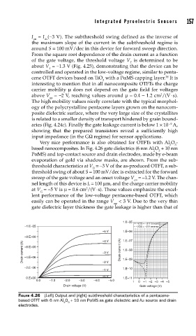
Very nice performance is also obtained for OTFTs with Al O -
2 3
based nanocomposites. In Fig. 4.26 gate dielectrics (6 nm Al O + 10 nm
2 3
PαMS) and top-contact source and drain electrodes, made by e-beam
evaporation of gold via shadow masks, are shown. From the sub-
threshold characteristics at V = −3 V of the as-produced OTFT, a sub-
D
threshold swing of about S = 100 mV/dec is extracted for the forward
sweep of the gate voltage and an onset voltage V = −1.2 V. The chan-
on
nel length of this device is L = 100 μm, and the charge carrier mobility
2
at V = −5 V is μ = 0.6 cm /(V ⋅ s). These values emphasize the excel-
G
lent performance of the low-voltage pentacene-based OTFT, which
easily can be operated in the range V < 3 V. Due to the very thin
op
gate dielectric layer thickness the gate leakage is higher than that of
1.E–05
VDS = –3 V forward
–1.E–05 VDS = –3 V reverse
–5 V 1.E–06
–8.E–06 –4 V 1.E–07
Drain current (A) –6.E–06 –3 V Drain current (A) 1.E–08
–4.E–06
1.E–09
–2.E–06 –2 V 1.E–10
–1 V
–0 V
0.E+00 1.E–11
0.0 –1.0 –2.0 –3.0 –4.0 –5.0 1 0 –1 –2 –3 –4 –5
Drain voltage (V) Gate voltage (V)
FIGURE 4.26 (Left) Output and (right) subthreshold characteristics of a pentacene-
based OTFT with 6 nm Al O + 10 nm PαMS as gate dielectric and Au source and drain
2 3
electrodes.