
Page 208 - Organic Electronics in Sensors and Biotechnology
P. 208
Progress and Challenges in OLED-Based Chemical and Biological Sensors 185
1.0
n-i-p
Normalized response 0.8 SiC barrier layer
0.9
0.7
0.6 p-i-n
0 5 10 15 20 25 30
Pulsed LED frequency (kHz)
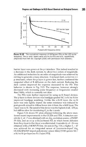
FIGURE 5.15 The normalized response of VHF-grown PDs vs the LED pulse
frequency. The p+ and i layers were a-Si/nc-Si/a-Si and a-Si, respectively.
(Reprinted from Ref. 64. Copyright 2008, with permission from Elsevier.)
barrier layer was grown at the p-i interface. This indeed resulted in
a decrease in the dark current, by about two orders of magnitude.
An additional reduction by an order of magnitude was achieved by
etching to generate a mesa structure. A reduced dark current in n-i-
p structures, where the p layer is grown last, further confirmed the
suspected effect of B diffusion on the dark current. Reducing the
dark current improved the response measured by the PD. This
behavior is shown in Fig. 5.15. The response, however, strongly
decreased with increasing pulse frequency at frequencies smaller
than 5 kHz, which is currently not clear.
The PDs were further improved by using nc-Si based devices.
The p layer in these devices was bandgap-graded SiC/a-Si/nc-Si for
improved bandgap matching. Unlike the a-Si:H layer, the nc-Si
layer was only lightly doped; the series resistance was reduced by
post-growth anneal to diffuse boron into it from the a-Si:H layer. The
i layer was nc-Si. The speed of this device was the highest of all, ~250 μs,
but still too slow for monitoring O in the τ mode.
2
Figure 5.16 shows SV plots obtained following the above men-
tioned recent improvements in the OLEDs and PDs. A detection sen-
sitivity S of ~7 was obtained with an Alq excitation source, a PtOEP:
g 3
PS film, and an n-i-p a-(Si,Ge)-based PD, in which boron diffusion
from the p layer to the i layer was eliminated. A sensitivity of ~26 was
obtained with a PdOEP:PS film. As seen in Fig. 5.16, a higher S ~ 47
g
was achieved for an integrated sensor of [coumarin-doped Alq
3
OLED]/[PdOEP-doped polystyrene sensor film]/[VHF-grown SiC/
a-Si/nc-Si (p+ layer):nc-Si (i layer) PD].