
Page 251 - Organic Electronics in Sensors and Biotechnology
P. 251
228 Cha pte r S i x
I B –
–
V OS
+
+
I B
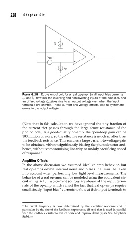
FIGURE 6.18 Equivalent circuit for a real op-amp. Small input bias currents
− +
I and I fl ow into the inverting and non-inverting inputs of the amplifi er, and
B B
an offset voltage V gives rise to an output voltage even when the input
OS
terminals are shorted. These current and voltage offsets lead to systematic
errors in the output voltage.
(Note that in this calculation we have ignored the tiny fraction of
the current that passes through the large shunt resistance of the
photodiode.) In a good-quality op-amp, the open-loop gain can be
100 million or more, so the effective resistance is much smaller than
the feedback resistance. This enables a large current-to-voltage gain
to be obtained without significantly biasing the photodetector and,
hence, without compromising linearity or unduly sacrificing speed
of response. †
Amplifier Offsets
In the above discussion we assumed ideal op-amp behavior, but
real op-amps exhibit internal noise and offsets that must be taken
into account when performing low light level measurements. The
behavior of a real op-amp can be modeled using the equivalent cir-
cuit in Fig. 6.18. Two current sources are shown at the input termi-
nals of the op-amp which reflect the fact that real op-amps require
small steady “input bias” currents to flow at their input terminals to
† The cutoff frequency is now determined by the amplifier response and in
particular by the size of the feedback capacitance (if any) that is used in parallel
with the feedback resistor to reduce noise and improve stability; see Sec. Amplifier
Stability.