Page 252 - Organic Electronics in Sensors and Biotechnology
P. 252
An Intr oduction to Or ganic Photodetectors     229

                                             -
                      51
               operate.  The input bias current i  at the inverting terminal is split
                                            B
               between the feedback resistor and the shunt resistance of the photo-
               diode in exactly the same way as the current i generated by the pho-
                                 -
               todiode. Therefore i  adds directly to i and experiences the same
                                 B
               transimpedance gain R , giving rise toa steady systematic offset DV  out
                                   f                                   ia
               in the output voltage:
                                             −
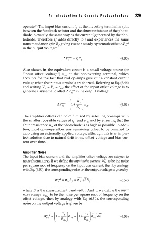
                                     ΔV out  =  i R                 (6.50)
                                        ia   B  f
               Also shown in the equivalent circuit is a small voltage source (or
               “input offset voltage”)  v  at the noninverting terminal, which
                                      OS
               accounts for the fact that real op-amps give out a constant output
               voltage when their input terminals are shorted. Referring to Eq. (6.46)
               and writing V  = V  = v , the effect of the input offset voltage is to
                           −
                                +
                                    OS
               generate a systematic offset DV  out  in the output voltage:
                                         va
                                         ⎛   R ⎞
                                  ΔV out  = ⎜ 1 +  f  ⎟  v          (6.51)
                                    va            OS
                                         ⎝   R sh⎠
               The amplifier offsets can be minimized by selecting op-amps with
                                           -
               the smallest possible values of i   and v  and by ensuring that the
                                           B      OS
               shunt resistance R  of the photodiode is as high as possible. In addi-
                               sh
               tion, most op-amps allow any remaining offset to be trimmed to
               zero using an externally applied voltage, although this is an imper-
               fect solution due to natural drift in the offset voltage and bias cur-
               rent over time.

               Amplifier Noise
               The input bias current and the amplifier offset voltage are subject to
               noise fluctuations. If we define the input noise current  σ   to be the noise
                                                            Ia
               per square root of frequency on the input bias current, then by analogy
               with Eq. (6.50), the corresponding noise on the output voltage is given by

                                             σ
                                 σ  out  =  σ R =     BR
                                  Ia    Ia  f  Ia   f               (6.52)
               where B is the measurement bandwidth. And if we define the input
               noise voltage σ    to be the noise per square root of frequency on the
                           Va
               offset voltage, then by analogy with Eq. (6.51), the corresponding
               noise on the output voltage is given by

                                ⎛   R ⎞      ⎛   R ⎞

                           σ out  = ⎜ 1 +  f  ⎟ σ  = ⎜ 1 +  f  ⎟ σ  B
                            Va           Va           Va            (6.53)
                                ⎝   R sh ⎠   ⎝   R sh⎠

