Page 253 - Organic Electronics in Sensors and Biotechnology
P. 253
230    Cha pte r  S i x

               In fact this last equation isn’t strictly correct because we have over-
                                                     †
               looked the capacitance C  of the photodiode.  This can be taken into
                                    d
               account by replacing the shunt resistance R  by the complex imped-
                                                    sh
               ance Z  = R | | Z , where Z  = 1/(j2πfC ). The capacitance introduces
                     sh  sh   C       C         d
               a frequency dependence into the gain, and after integrating over all
               frequencies (see the Appendix), the root mean squared noise voltage
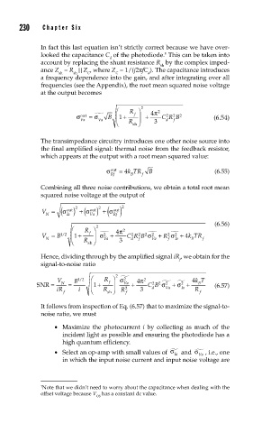
               at the output becomes
                                       ⎛  R ⎞ 2   π  2
                          σ  out  =     B ⎜ 1  +  f  ⎟ +  4  CR B 2  (6.54)
                                σ
                                                      2
                                                        2
                           Va    Va                   d  f
                                       ⎝  R sh⎠   3
               The transimpedance circuitry introduces one other noise source into
               the final amplified signal: thermal noise from the feedback resistor,
               which appears at the output with a root mean squared value:
                                   σ out  = 4 kTR  B                (6.55)
                                     Rf    B  f
               Combining all three noise contributions, we obtain a total root mean
               squared noise voltage at the output of
                V = ( ) +( ) +( )       2
                          2
                                 2
                             σ
                                    σ
                      σ
                       out
                              out
                                      out
                 N     Ia     Va      Rf
                                                                    (6.56)
                         ⎛   R ⎞  2   4π 2
                                               2
                                                      2
                                                          +
                V =  B 12  1 ⎜  +  f  ⎟ σ 2   +  CR B σ 2  +  R σ + 4kTR
                                                        2
                                           2
                                             2
                      /
                 N                 Va      d  f  Va   f  Ia  B   f
                         ⎝   R R sh⎠   3
               Hence, dividing through by the amplified signal iR , we obtain for the
                                                          f
               signal-to-noise ratio
                                      2
                           /
                    V     B 12  ⎛  R  f  ⎞ σ 2    4π 2  2    2    4 kT
              SNR =   N  =     ⎜ 1 +  ⎟  Va  +  C B σ  2  + σ +  B  (6.57)
                                                 2
                    iR     i   ⎝  R sh⎠  R 2  3  d d  Va  Ia  R
                      f                  f                      f
               It follows from inspection of Eq. (6.57) that to maximize the signal-to-
               noise ratio, we must
                    •  Maximize the photocurrent  i by collecting as much of the
                      incident light as possible and ensuring the photodiode has a
                      high quantum efficiency.
                    •  Select an op-amp with small values of  σ    Va
                                                        Ia  and  σ   , i.e., one
                      in which the input noise current and input noise voltage are
               † Note that we didn’t need to worry about the capacitance when dealing with the
               offset voltage because V  has a constant dc value.
                                OS

