
Page 273 - Organic Electronics in Sensors and Biotechnology
P. 273
250 Cha pte r S i x
Light scattering
ITO
Transport layer
Conduction
Generation layer
Contact pad Gap
Organic sensor
Passivation
TFT Capacitor
Substrate
(a) (b)
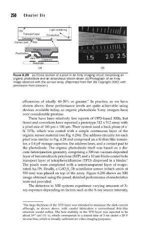
FIGURE 6.29 (a) Cross section of a pixel in an X-ray imaging circuit comprising an
organic photodiode and an amorphous silicon driver. (b) Photograph of an X-ray
image obtained with the sensor array. (Reprinted from Ref. 88. Copyright 2002, with
permission from Elsevier.)
efficiencies of ideally 40–50% or greater.” In practice, as we have
shown above, these performance levels are quite achievable using
devices available today, so organic photodiode X-ray imagers have
very considerable promise.
There have been relatively few reports of OPD-based XRIs, but
Street and coworkers have reported a prototype 512 × 512 array with
a pixel size of 100 μm × 100 μm. Their system used a back plane of a-
Si TFTs, which was coated with a simple continuous layer of the
organic sensor material (see Fig. 6.29a). The address circuitry for each
pixel was similar to Fig. 6.28 and comprised an a-Si thin film transis-
tor, a 0.4 pF storage capacitor, the address lines, and a contact pad to
the photodiode. The organic photodiode itself was based on a dis-
crete heterojunction geometry, comprising a 300 nm vacuum-deposited
layer of benzimidazole perylene (BZP) and a 10 μm blade-coated hole
transport layer of tetraphenyldiamine (TPD) dispersed in a binder. †
The pixels were completed with a semitransparent layer of evapo-
rated Au/Pt. Finally, a GdO S :Tb scintillator screen (which emits at
2 2
550 nm) was placed on top of the array. Figure 6.29b shows an XRI
image obtained using the panel; detailed performance characteristics
were not provided.
The detectors in XRI systems experience varying amounts of X-
ray exposure depending on factors such as the X-ray source intensity,
† The large thickness of the TPD layer was intended to minimize the dark current
although, as shown above, with careful fabrication a conventional thin-film
structure would suffice. The hole mobility in the TPD layer was reported to be
.
−5
2
about 10 cm /(V s), which corresponds to a transit time of 3 ms under a 20 V
reverse bias, which is broadly sufficient for video imaging purposes.