
Page 271 - Organic Electronics in Sensors and Biotechnology
P. 271
248 Cha pte r S i x
complexity of the fabrication process, the panels are expensive, and
there is significant interest in alternative technologies that would per-
mit larger panels to be fabricated at substantially reduced cost.
OPV devices are especially appealing in this respect due to their
excellent optoelectronic characteristics and their amenability to large-area,
low-cost printing. The use of flexible plastic substrates raises the possi-
bility of creating low-cost, large-area conformable panels that can adapt
to the shape of the object or the radiation source, offering superior reso-
lution and imaging capabilities. With these benefits in mind, Blakesley
87
and Speller undertook a conceptual feasibility study to determine
whether OPV panels could provide a viable alternative to existing panel
87
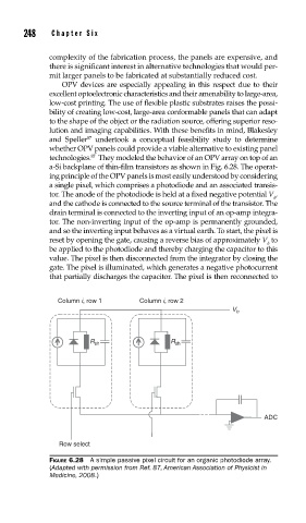
technologies. They modeled the behavior of an OPV array on top of an
a-Si backplane of thin-film transistors as shown in Fig. 6.28. The operat-
ing principle of the OPV panels is most easily understood by considering
a single pixel, which comprises a photodiode and an associated transis-
tor. The anode of the photodiode is held at a fixed negative potential V ,
b
and the cathode is connected to the source terminal of the transistor. The
drain terminal is connected to the inverting input of an op-amp integra-
tor. The non-inverting input of the op-amp is permanently grounded,
and so the inverting input behaves as a virtual earth. To start, the pixel is
reset by opening the gate, causing a reverse bias of approximately V to
b
be applied to the photodiode and thereby charging the capacitor to this
value. The pixel is then disconnected from the integrator by closing the
gate. The pixel is illuminated, which generates a negative photocurrent
that partially discharges the capacitor. The pixel is then reconnected to
Column i, row 1 Column i, row 2
V b
R sh R sh
ADC
Row select
FIGURE 6.28 A simple passive pixel circuit for an organic photodiode array.
(Adapted with permission from Ref. 87, American Association of Physicist in
Medicine, 2008.)