Page 272 - Organic Electronics in Sensors and Biotechnology
P. 272
An Intr oduction to Or ganic Photodetectors     249

               the integrator by opening the gate, and the photodiode capacitor is
               recharged to a value V . This requires an amount Q of charge to flow
                                  b
               that––assuming an ideal transistor with infinite off resistance and zero
               on resistance––is equal to the charge generated by the photodiode. The
               integrator generates an output voltage that is proportional to Q, which is
               then read using an analog-to-digital converter (ADC). The panel oper-
               ates in a similar way, except there is one integrator/ADC for each col-
               umn of the array, and the pixels are read on a row-by-row basis. The
               pixels are first reset by opening and closing their gates. They are then
               briefly illuminated with the X-ray image. The pixels in the first row are
               selected by opening their gates and read as described above. The first
               row is deselected, and the read process is repeated for each row in turn.
                   The dark current is an important source of error in photodiode
               sensor arrays. There is a delay between resetting each pixel and read-
               ing its charge, during which a dark current will flow; each photodi-
               ode is reverse-biased, so the dark current flows in the same direction
               as the photocurrent and leads to faster discharging of the pixels. To
               correct for this effect, the measurement can be repeated in the dark
               and the background count subtracted from the signal count. This pro-
               cedure is valid, however, only if the dark currents are the same for the
               two measurements. In reality, the dark current changes continuously
               as the capacitor discharges and the device bias diminishes. A signifi-
               cant change in the device bias would also reduce the quantum effi-
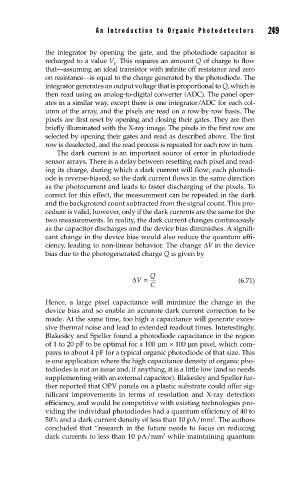
               ciency, leading to non-linear behavior. The change ΔV in the device
               bias due to the photogenerated charge Q is given by


                                            Q
                                       ΔV =                         (6.71)
                                            C
               Hence, a large pixel capacitance will minimize the change in the
               device bias and so enable an accurate dark current correction to be
               made. At the same time, too high a capacitance will generate exces-
               sive thermal noise and lead to extended readout times. Interestingly,
               Blakesley and Speller found a photodiode capacitance in the region
               of 1 to 20 pF to be optimal for a 100 μm × 100 μm pixel, which com-
               pares to about 4 pF for a typical organic photodiode of that size. This
               is one application where the high capacitance density of organic pho-
               todiodes is not an issue and, if anything, it is a little low (and so needs
               supplementing with an external capacitor). Blakesley and Speller fur-
               ther reported that OPV panels on a plastic substrate could offer sig-
               nificant improvements in terms of resolution and X-ray detection
               efficiency, and would be competitive with existing technologies pro-
               viding the individual photodiodes had a quantum efficiency of 40 to
                                                             2
               50% and a dark current density of less than 10 pA/mm . The authors
               concluded that “research in the future needs to focus on reducing
                                                2
               dark currents to less than 10 pA/mm  while maintaining quantum

