
Page 267 - Organic Electronics in Sensors and Biotechnology
P. 267
244 Cha pte r S i x
6.7 Technology and Applications
In this final section, we consider some of the applications to which
organic photodiodes have so far been applied. This list is in no sense
intended to be exhaustive, and given the vast number of uses to
which photodetectors have historically been put, it is inevitable that
many new applications will be found in the coming years.
6.7.1 Printed and Flexible Devices
The ability to process conjugated polymers (and an increasing number
of small molecules) from solution opens up considerable opportunities
for cost savings, relative to conventional inorganic semiconductors.
The usual method for “one-off” laboratory-scale device fabrication is
spin-coating, a very reliable process that yields high-quality uniform
films but involves significant materials wastage. The on-demand
nature of printing methods results in efficient materials usage and
offers an attractive means of making complex structures such as
one- and two-dimensional sensor arrays. The most developed tech-
nique for organic semiconductor devices is inkjet printing, in which
a small droplet of solvent containing the active materials is pro-
pelled from a chamber or head usually by piezoelectric expansion.
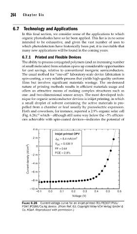
Hoth and coworkers, for instance, reported a 2.9% organic solar cell
63
(Fig. 6.26), which—although still some way below the ~5% efficien-
cies achievable with spin-coated devices—indicates the potential of
4 m
Inkjet printed OPV
2 m J SC = 8.4 mA/cm 2
V OC = 0.535 V
Current density (A/cm 2 ) –2 m PCE = 2.9%
0
FF = 0.64
–4 m
–6 m
–8 m
–10 m
–0.1 0.0 0.1 0.2 0.3 0.4 0.5 0.6
Voltage (V)
FIGURE 6.26 Current-voltage curve for an inkjet-printed ITO/PEDOT:PSS/
P3HT:PCBM/Ca:Ag device. (From Ref. 63. Copyright Wiley-VCH Verlag GmbH &
Co. KGaA. Reproduced with permission.)