
Page 262 - Organic Electronics in Sensors and Biotechnology
P. 262
An Intr oduction to Or ganic Photodetectors 239
10 1
10 0 @ 560 nm
10 –1
Current density (mA/cm 2 ) 10 –3
–2
10
–4
10
–5
10
–6
10
10
Photocurrent
–8
10 –7 Dark current
10 –9
–1.0 –0.8 –0.6 –0.4 –0.2 0.0 0.2 0.4 0.6 0.8 1.0
Voltage (V)
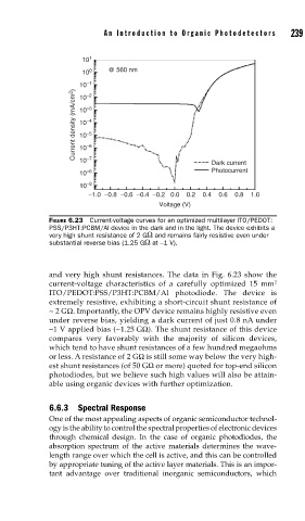
FIGURE 6.23 Current-voltage curves for an optimized multilayer ITO/PEDOT:
PSS/P3HT:PCBM/Al device in the dark and in the light. The device exhibits a
very high shunt resistance of 2 GΩ and remains fairly resistive even under
substantial reverse bias (1.25 GΩ at −1 V).
and very high shunt resistances. The data in Fig. 6.23 show the
current-voltage characteristics of a carefully optimized 15 mm 2
ITO/PEDOT:PSS/P3HT:PCBM/Al photodiode. The device is
extremely resistive, exhibiting a short-circuit shunt resistance of
~ 2 GΩ. Importantly, the OPV device remains highly resistive even
under reverse bias, yielding a dark current of just 0.8 nA under
−1 V applied bias (~1.25 GΩ). The shunt resistance of this device
compares very favorably with the majority of silicon devices,
which tend to have shunt resistances of a few hundred megaohms
or less. A resistance of 2 GΩ is still some way below the very high-
est shunt resistances (of 50 GΩ or more) quoted for top-end silicon
photodiodes, but we believe such high values will also be attain-
able using organic devices with further optimization.
6.6.3 Spectral Response
One of the most appealing aspects of organic semiconductor technol-
ogy is the ability to control the spectral properties of electronic devices
through chemical design. In the case of organic photodiodes, the
absorption spectrum of the active materials determines the wave-
length range over which the cell is active, and this can be controlled
by appropriate tuning of the active layer materials. This is an impor-
tant advantage over traditional inorganic semiconductors, which