
Page 261 - Organic Electronics in Sensors and Biotechnology
P. 261
238 Cha pte r S i x
Failure to adequately address these issues can result in disas-
−4
trously high shunt conductances of 10 S or more. With care, though,
it is possible to reduce shunt conductances below the 10 S level,
−8
corresponding to shunt resistances in excess of 100 MΩ. At this
level, the residual conductance is most probably due to current
flow through the active layer rather than shunts. In many OPV
devices, ohmic contacts are present at one or both electrodes (since
this maximizes the built-in field and is therefore beneficial for the
quantum efficiency [see Eq. (6.5)]. In such situations, appreciable
injection can occur from the electrodes into the active layer materi-
als even at very low biases. This is especially problematic for bulk
heterojunction devices where the donor and acceptor materials
can make continuous percolation pathways from one electrode to
the other, providing effective shunts for injected holes and elec-
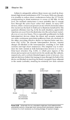
trons (Fig. 6.22a). (In discrete heterojunction devices, injected
charges are blocked at the heterojunction, resulting in low dark
currents and high shunt resistances.) The simplest way to mini-
mize the dark current in bulk heterojunction devices is to use a
three-layer structure (Fig. 6.22b), in which pure regions of the
donor and acceptor are located next to the anode and the cathode,
respectively, and a uniform blended region exists in between. Any
injected electrons (holes) that manage to pass through the bulk of the
device are blocked on reaching the donor (acceptor) layer adjacent
to the anode (cathode), resulting in extremely low dark currents
p type
p type n type surface layer n type
(b)
Anode Cathode
Continuous
shunt between
two electrodes
(a)
FIGURE 6.22 Schematic for (a) a standard single-layer bulk heterojunction
photodiode and (b) a three-layer bulk heterojunction photodiode designed to
minimize the shunt resistance by blocking leakage of injected charges.