Page 260 - Organic Electronics in Sensors and Biotechnology
P. 260
An Intr oduction to Or ganic Photodetectors     237

               determined a 1 MHz cutoff frequency at −5 V from the Fourier trans-
               form of the impulse response (Fig. 6.21). This was limited by the slow
               turnoff characteristics of the device, and the fast turn-on characteris-
               tics suggest significantly faster response is in principle possible; based
               on the < 2 ns rise time, a cutoff frequency of order 100 MHz would be
               expected.


               6.6.2 Shunt Resistance
               As discussed above, the shunt resistance influences both the thermal
               noise of the photodiode and the output noise voltage from the ampli-
               fier, with it being important in both cases to maximize the shunt resis-
               tance in order to minimize the noise. In this section, we will consider
               how the shunt resistance of an OPV device can be maximized,
               although we will find it more convenient to couch our discussion in
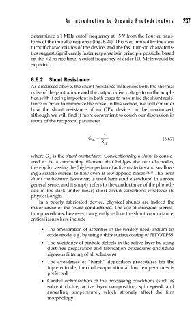
               terms of the reciprocal parameter

                                             1
                                      G   =                         (6.67)
                                        sh
                                            R
                                             sh
               where G  is the shunt conductance. Conventionally, a shunt is consid-
                       sh
               ered to be a conducting filament that bridges the two electrodes,
               thereby bypassing the (high-impedance) active materials and so allow-
               ing a sizable current to flow even at low applied biases. 54, 55  The term
               shunt conductance, however, is used here (and elsewhere) in a more
               general sense, and it simply refers to the conductance of the photodi-
               ode in the dark under (near) short-circuit conditions whatever its
               physical origin.
                   In a poorly fabricated device, physical shunts are indeed the
               major cause of the shunt conductance. The use of stringent fabrica-
               tion procedures, however, can greatly reduce the shunt conductance;
               critical issues here include

                    •  The amelioration of asperities in the (widely used) indium tin
                      oxide anode, e.g., by using a thick surface coating of PEDOT:PSS
                    •  The avoidance of pinhole defects in the active layer by using
                      dust-free preparation and fabrication procedures (including
                      rigorous filtering of all solutions)
                    •  The avoidance of “harsh” deposition procedures for the
                      top electrode; thermal evaporation at low temperatures is
                      preferred
                    •  Careful optimization of the processing conditions (such as
                      solvent choice, active layer composition, spin speed, and
                      annealing temperature), which strongly affect the film
                      morphology

