
Page 259 - Organic Electronics in Sensors and Biotechnology
P. 259
236 Cha pte r S i x
time required for the photogenerated charge carriers to pass through
the thickness of the device. The transit time can be estimated from the
drift velocity v = μE of the slowest charge carriers where μ is the
mobility and E = (V - V )/d is the internal field strength. The transit
BI
time is therefore equal to
d d d 2
τ = = = (6.66)
|
v [ μE] μ V − V |
BI
In the non-RC-limited regime, a device is expected to reach steady
state within a few transit times, and hence the speed of response is
maximized by using thin devices under a significant reverse bias.
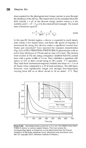
53
Punke and coworkers have reported the transient characteristics
(Fig. 6.21) of ITO/PEDOT:PSS/P3HT:PCBM/Al photodiodes with an
2
active layer thickness of 170 nm and an area of 0.2 mm . The devices
were excited at 532 nm using a frequency doubled Nd:YAG pulsed
laser with a pulse width of 1.6 ns. They exhibited a quantum effi-
ciency of 12% at short circuit rising to 34% under -5 V operation.
They had short (instrument-response limited) rise times of < 2 ns at
all biases when connected to a 25 Ω load resistance. The fall times,
however, were significantly longer and strongly bias-dependent,
varying from 426 ns at short circuit to 36 ns under −5 V. They
1.0 0
0.8 Normalized response (dB) –10
Normalized response 0.6 –30 10 6 0 V Bias voltage: –5 V 8
–20
7
10
10
Frequency (Hz)
0.4
–1 V
0.2
0.0
0 100 200 300 400 500 600 700
Time (ns)
2
FIGURE 6.21 Normalized pulse curves for a 0.2 mm ITO/PEDOT:PSS/P3HT:
PCBM/Al device at various applied biases. The inset shows the
corresponding signal vs.frequency curves determined from the Fourier
transform of the pulse response curve. (Reprinted with permission from
Ref. 53. Copyright 2007, American Institute of Physics.)