
Page 266 - Organic Electronics in Sensors and Biotechnology
P. 266
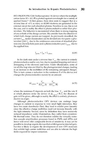
An Intr oduction to Or ganic Photodetectors     243

               ITO/PEDOT:PSS/C60/bathocuproine/Al device where the multipli-
               cation factor M = ΔI/eℜ is plotted against wavelength for a variety of
                            61
               applied biases.  At first glance, these data seem to suggest that at a
               reverse bias of -4 V, as many as 40,000 electrons are generated in the
               external circuit for each absorbed photon. Needless to say, this is not
               the case, and in reality the effect is photoconductive rather than pho-
               tovoltaic. The behavior is encountered when there is strong trapping
               of one or both of the charge carriers. We consider here the situation in
               which both charge carriers are trapped. As previously described, the
               current I   under illumination can be divided into two parts: a pho-
                       photo
               tovoltaic part I  due to the continuous conversion of absorbed pho-
                            ph
               tons into electron-hole pairs and a photoconductive part I    due to
                                                               Vphoto
               the applied bias.
                                   I   +  I  +  I                   (6.69)
                                    photo  ph  V photo

                   In the dark state under a reverse bias V , the current is entirely
                                                    rev
               photoconductive and is very low due to repeated trapping and (slow)
               detrapping of the electrons and holes. Under illumination, some of
               (or all) the trap sites are filled by the photogenerated charges, leading
               to an increase in the mobilities of the remaining untrapped charges.
               This in turn causes a reduction in the resistance R of the device and
               changes the photoconductive current by an amount


                                        V         V
                             ΔI     =    rev  −    rev              (6.70)
                               V photo
                                       (
                                                 (
                                      RV , )0   RV , ℜ)
                                         rev       rev
               where the resistance R depends on both the bias  V  and the rate ℜ
                                                           rev
               at which photons strike the device: if  ΔI  >ℜ/e, the illusion of
                                                   V  photo
               gain will be given, although in reality the effect is entirely photocon-
               ductive in origin.
                   Although photoconductive OPV devices can undergo large
               changes in current in response to very small light intensities, they
               have two main drawbacks: First, they tend to exhibit poor linearity
               since the effective charge mobilities need not increase linearly with
               the light intensity. Second, since by definition they have massively
               reduced impedance under illumination, they suffer from considera-
               ble thermal noise. They do not therefore exhibit the virtually noise-
               free cascade amplification processes found in PMTs and APDs and
               hence will never offer comparable levels of sensitivity. It may yet be
               possible to develop organic devices that exhibit genuine internal gain,
               but this is likely to require the development of new OPV materials
               that exhibit high carrier mobilities and are able to tolerate the high
               fields required for impact ionization.