
Page 270 - Organic Electronics in Sensors and Biotechnology
P. 270
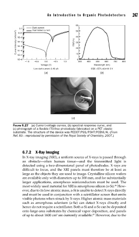
An Intr oduction to Or ganic Photodetectors     247

                                             60
              0.1    Dark current            50
                     Illuminated current
            Current density (mA/cm 2 )  1E–3  EQE(%)  40
             0.01
             1E–4
                                             30
             1E–5
                                             20
             1E–6
             1E–7                            10
             1E–8                             0
                 –1.0  –0.5  0.0  –0.5  1.0   300  400  500  600  700  800
                          Voltage (V)                  Wavelength (nm)
                      Low dark current: 0.46 pA      EQE >55% el/ph@ 0 V
                            (a)                            (b)


                                           (c)

          FIGURE 6.27  (a) Current-voltage curves, (b) spectral response curve, and
          (c) photograph of a fl exible ITO-free photodiode fabricated on a PET plastic
          substrate. The structure of the device was PEDOT:PSS/P3HT:PCBM/Al. (From
          Ref. 83—reproduced by permission of the Royal Society of Chemistry, 2007.)


               6.7.2 X-Ray Imaging
               In X-ray imaging (XRI), a uniform source of X-rays is passed through
               an obstacle––often human tissue––and the transmitted light is
               detected using a two-dimensional panel of photodiodes. X-rays are
               difficult to focus, and the XRI panels must therefore be at least as
               large as the objects they are used to image. Crystalline silicon wafers
               are available only with diameters up to 300 mm, and for substantially
               larger applications, amorphous semiconductors must be used. The
                                                                   86
               most widely used material for XRI is amorphous silicon (a-Si).  How-
               ever, due to its low atomic mass, a-Si is unable to detect X-rays directly
               and must be used in conjunction with a scintillator screen that emits
               visible photons when struck by X-rays. Higher atomic mass materials
               such as amorphous selenium (a-Se) can detect X-rays directly and
               hence do not require a scintillator. Both a-Si and a-Se can be deposited
               onto large-area substrates by chemical vapor deposition, and panels
                                                      87
               of up to about 1600 cm  are currently available.  However, due to the
                                  2