
Page 275 - Organic Electronics in Sensors and Biotechnology
P. 275
252 Cha pte r S i x
interact with glass, and it was suggested that improved stability
against might be achieved using plastic substrates. The other two
material systems exhibited a remarkable tolerance to X-ray exposure,
and it is apparent from these studies that organic materials are able
to withstand the lifetime X-ray doses experienced in standard XRI
applications.
Although we have focused here on XRI applications, there are a
number of other applications where large-area imagers would be of
value. The most obvious, perhaps, is document scanning where an
extended 2D image sensor offers the possibility of faster image acqui-
sition than conventional moving 1D scanners, while also removing
the need for mechanical parts. Other applications where large-area
scanners could be of great utility are X-ray crystallography and neu-
tron detection, the latter being widely used in industry to detect cor-
rosion. The above 2D sensors used amorphous silicon back panels to
address the pixels, and hence did not make full use of the low-cost
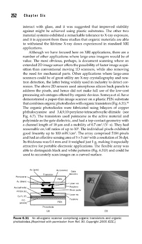
processing advantages offered by organic devices. Someya et al. have
demonstrated a paper-thin image scanner on a plastic PEN substrate
that combines organic photodiodes with organic transistors (Fig. 6.31). 90
The organic photodiodes were fabricated using bilayers of copper
phthalocyanine and 3,4,9,10-perylene-tetracarboxylic-diimide (see
Fig. 6.7). The transistors used pentacene as the active material and
polyimide as the gate dielectric, and had a top-contact geometry with
a channel length of 18 μm and a mobility of 0.7 cm /(V . s). They had
2
reasonable on/off ratios of up to 10 . The individual pixels exhibited
5
2
good linearity up to 100 mW/cm . The array comprised 5184 pixels
2
and had an effective sensing area of 5 × 5 cm with a resolution of 36 dpi.
Its thickness was 0.4 mm and it weighed just 1 g, making it especially
attractive for portable electronic applications. The flexible array was
able to distinguish black and white patterns (Fig. 6.31b) and could be
used to accurately scan images on a curved surface.
Au (gate) Au (source)
Gate
Transistor dielectric
Pentacene
PEN
Au (drain)
Laser via
Au (cathode) Parylene
Silver paste
PTCDI (N)
Laser via
CuPc (P)
Parylene
ITO
(anode) PEN
Photodiode
(a) (b)
FIGURE 6.31 An all-organic scanner comprising organic transistors and organic
photodiodes.(Reprinted with permission from Ref. 90. Copyright 2005 IEEE.)