
Page 294 - Organic Electronics in Sensors and Biotechnology
P. 294
Organic Semiconductor Lasers as Integrated Light Sources for Optical Sensors 271
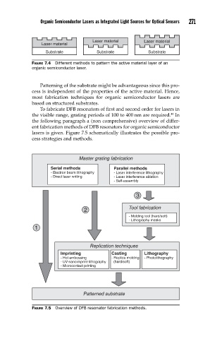
Laser material Laser material
Laser material
Substrate Substrate Substrate
FIGURE 7.4 Different methods to pattern the active material layer of an
organic semiconductor laser.
Patterning of the substrate might be advantageous since this pro-
cess is independent of the properties of the active material. Hence,
most fabrication techniques for organic semiconductor lasers are
based on structured substrates.
To fabricate DFB resonators of first and second order for lasers in
40
the visible range, grating periods of 100 to 400 nm are required. In
the following paragraph a (non comprehensive) overview of differ-
ent fabrication methods of DFB resonators for organic semiconductor
lasers is given. Figure 7.5 schematically illustrates the possible pro-
cess strategies and methods.
Master grating fabrication
Serial methods Parallel methods
- Electron beam lithography - Laser interference lithography
- Direct laser writing - Laser interference ablation
- Self-assembly
3
2 Tool fabrication
- Molding tool (hard/soft)
- Lithography masks
1
Replication techniques
Imprinting Casting Lithography
- Hot embossing - Replica molding - Photolithography
- UV-nanoimprint-lithography (hard/soft)
- Microcontact printing
Patterned substrate
FIGURE 7.5 Overview of DFB resonator fabrication methods.