
Page 295 - Organic Electronics in Sensors and Biotechnology
P. 295
272 Chapter Seven
There are three main process chains that lead to a DFB resonator
grating substrate. Each process chain includes structuring of a master
substrate. In the first process chain (1) this master is directly used as
laser substrate. However, the fabrication of a master substrate is
expensive and time-consuming, thus this method is only used for
prototyping. A second process chain (2) uses the replication of the
master substrate. Different methods allow the multiple replication
with the master substrate used as a molding tool. However, the mas-
ter itself may be damaged during the process. This is avoided by
introducing the fabrication of a replication tool (3) which can be opti-
mized for long durability. Thus, the latter process chain is suited best
for commercial applications.
The master substrate can be fabricated by serial or parallel pro-
cesses. Serial processes such as electron beam lithography or direct
laser writing allow for highest freedom in design of the structures. In
comparison, parallel processes such as laser interference lithography
or ablation are fast and applicable to large areas. In the following we
will describe the most important fabrication methods for the master.
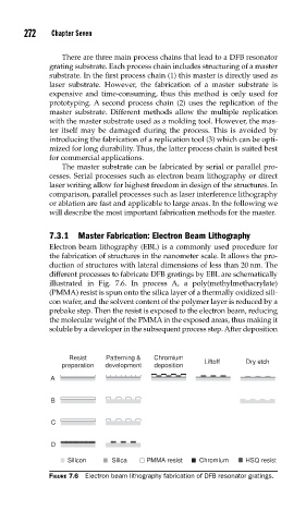
7.3.1 Master Fabrication: Electron Beam Lithography
Electron beam lithography (EBL) is a commonly used procedure for
the fabrication of structures in the nanometer scale. It allows the pro-
duction of structures with lateral dimensions of less than 20 nm. The
different processes to fabricate DFB gratings by EBL are schematically
illustrated in Fig. 7.6. In process A, a poly(methylmethacrylate)
(PMMA) resist is spun onto the silica layer of a thermally oxidized sili-
con wafer, and the solvent content of the polymer layer is reduced by a
prebake step. Then the resist is exposed to the electron beam, reducing
the molecular weight of the PMMA in the exposed areas, thus making it
soluble by a developer in the subsequent process step. After deposition
Resist Patterning & Chromium
Liftoff Dry etch
preparation development deposition
A
B
C
D
Silicon Silica PMMA resist Chromium HSQ resist
FIGURE 7.6 Electron beam lithography fabrication of DFB resonator gratings.