
Page 123 - PDA Robotics Using Your Personal Digital Assistant to Control Your Robot
P. 123
PDA 05 5/30/03 11:35 AM Page 99
Chapter 5 / The Electronics
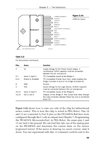
Figure 5.44
L298 pin layout.
Table 5.5
Pin Descriptions (continued)
Pins Name Function
4 Vs Supply Voltage for the Power Output stages. A
noninductive 100nF capacitor must be connected
between this pin and ground.
5,7 Input 1; Input 2 TTL Compatible Inputs of the Bridge A.
6,11 Enable A; EnableB TTL Compatible Enable Input: the L state disables the
bridge A (enable A) and/or the bridge B (enable B).
8 GND Ground.
9 VSS Supply Voltage for the Logic Blocks. A100nF capacitor
must be connected between this pin and ground.
10,12 Input 3; Input 4 TTL Compatible Inputs of the Bridge B.
13,14 Out 3; Out 4 Outputs of the Bridge B. The current that flows through
the load connected between these two pins is monitored
at pin 15.
Figure 5.45 shows how to wire one side of the chip for bidirectional
motor control. This is how the chip is wired in PDA Robot. Pins 10
and 12 are connected to Port B pins on the PIC16F876 that have been
configured through the C code as outputs (see Chapter 7: Programming
the PIC16F876 Microcontroller). In PDA Robot, the sense pins 1 and
15 are tied to the ground. We can feed this into one of the analog pins
on the PIC16F876 and determine the current draw on the motors
(explained below). If the motor is drawing too much current, shut it
down. You can experiment with this. A command could be sent to the
99