
Page 119 - PDA Robotics Using Your Personal Digital Assistant to Control Your Robot
P. 119
PDA 05 5/30/03 11:35 AM Page 95
Chapter 5 / The Electronics
CLKOUT (= osc/4)
Data Bus
8
0 M 1
RA4/TOCKI U M Sync
pin X U 2 TMR0 Reg
1 0
X Cycles
TOSE
TOCS
PSA Set Flag Bit T0IF
on Overflow
Prescaler
0
8-bit Prescaler
M
U
1 X 8
Watchdog
Timer
8- - to 1-MUX PS2:PS0
PSA
0 1
WDT Enable bit
MUX PSA
WDT
Time-out
Note: TOCS, TOSE, PSA, PS2:PS0 are (OPTION_REG<5:0>.
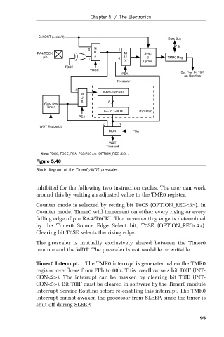
Figure 5.40
Block diagram of the Timer0/WDT prescaler.
inhibited for the following two instruction cycles. The user can work
around this by writing an adjusted value to the TMR0 register.
Counter mode is selected by setting bit T0CS (OPTION_REG<5>). In
Counter mode, Timer0 will increment on either every rising or every
falling edge of pin RA4/T0CKI. The incrementing edge is determined
by the Timer0 Source Edge Select bit, T0SE (OPTION_REG<4>).
Clearing bit T0SE selects the rising edge.
The prescaler is mutually exclusively shared between the Timer0
module and the WDT. The prescaler is not readable or writable.
Timer0 Interrupt. The TMR0 interrupt is generated when the TMR0
register overflows from FFh to 00h. This overflow sets bit T0IF (INT-
CON<2>). The interrupt can be masked by clearing bit T0IE (INT-
CON<5>). Bit T0IF must be cleared in software by the Timer0 module
Interrupt Service Routine before re-enabling this interrupt. The TMR0
interrupt cannot awaken the processor from SLEEP, since the timer is
shut-off during SLEEP.
95