
Page 115 - PDA Robotics Using Your Personal Digital Assistant to Control Your Robot
P. 115
PDA 05 5/30/03 11:35 AM Page 91
Chapter 5 / The Electronics
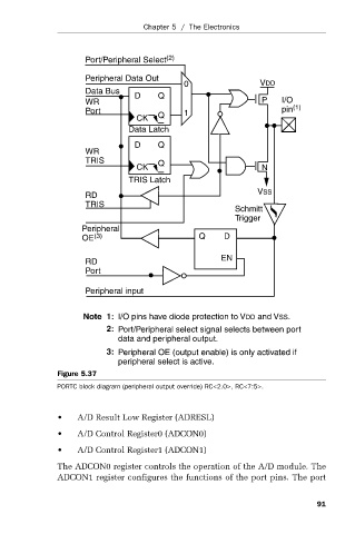
Port/Peripheral Select (2)
Peripheral Data Out
0 VDD
Data Bus
D Q
WR P I/O
Port 1 pin (1)
CK Q
Data Latch
D Q
WR
TRIS Q
CK N
TRIS Latch
RD VSS
TRIS
Schmitt
Trigger
Peripheral
OE (3) Q D
EN
RD
Port
Peripheral input
Note 1: I/O pins have diode protection to VDD and VSS.
2: Port/Peripheral select signal selects between port
data and peripheral output.
3: Peripheral OE (output enable) is only activated if
peripheral select is active.
Figure 5.37
PORTC block diagram (peripheral output override) RC<2.0>, RC<7:5>.
• A/D Result Low Register (ADRESL)
• A/D Control Register0 (ADCON0)
• A/D Control Register1 (ADCON1)
The ADCON0 register controls the operation of the A/D module. The
ADCON1 register configures the functions of the port pins. The port
91