
Page 110 - PDA Robotics Using Your Personal Digital Assistant to Control Your Robot
P. 110
PDA 05 5/30/03 11:35 AM Page 86
Data Data Latch PDA Robotics
Bus
D Q
WR
Port
CK Q
I/O pin (1)
N
TRIS Latch
D Q
VSS
WR
TRIS
CK Q Schmitt
Trigger
Input
Buffer
RD
TRIS
Q D
EN
RD Port
TMR0 Clock Input
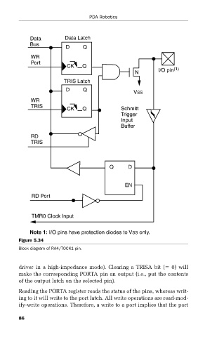
Note 1: I/O pins have protection diodes to VSS only.
Figure 5.34
Block diagram of RA4/TOCK1 pin.
driver in a high-impedance mode). Clearing a TRISA bit ( 0) will
make the corresponding PORTA pin an output (i.e., put the contents
of the output latch on the selected pin).
Reading the PORTA register reads the status of the pins, whereas writ-
ing to it will write to the port latch. All write operations are read-mod-
ify-write operations. Therefore, a write to a port implies that the port
86