
Page 108 - PDA Robotics Using Your Personal Digital Assistant to Control Your Robot
P. 108
PDA 05 5/30/03 11:35 AM Page 84
PDA Robotics
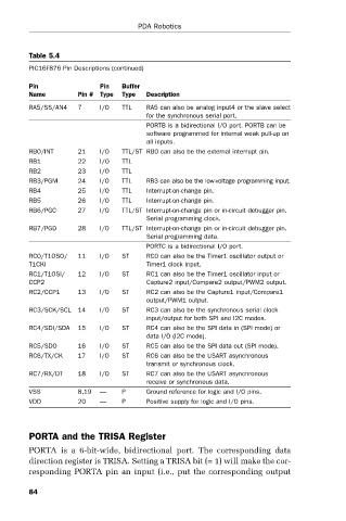
Table 5.4
PIC16F876 Pin Descriptions (continued)
Pin Pin Buffer
Name Pin # Type Type Description
RA5/SS/AN4 7 I/O TTL RA5 can also be analog input4 or the slave select
for the synchronous serial port.
PORTB is a bidirectional I/O port. PORTB can be
software programmed for internal weak pull-up on
all inputs.
RB0/INT 21 I/O TTL/ST RB0 can also be the external interrupt pin.
RB1 22 I/O TTL
RB2 23 I/O TTL
RB3/PGM 24 I/O TTL RB3 can also be the low-voltage programming input.
RB4 25 I/O TTL Interrupt-on-change pin.
RB5 26 I/O TTL Interrupt-on-change pin.
RB6/PGC 27 I/O TTL/ST Interrupt-on-change pin or in-circuit debugger pin.
Serial programming clock.
RB7/PGD 28 I/O TTL/ST Interrupt-on-change pin or in-circuit debugger pin.
Serial programming data.
PORTC is a bidirectional I/O port.
RC0/T1OSO/ 11 I/O ST RC0 can also be the Timer1 oscillator output or
T1CKI Timer1 clock input.
RC1/T1OSI/ 12 I/O ST RC1 can also be the Timer1 oscillator input or
CCP2 Capture2 input/Compare2 output/PWM2 output.
RC2/CCP1 13 I/O ST RC2 can also be the Capture1 input/Compare1
output/PWM1 output.
RC3/SCK/SCL 14 I/O ST RC3 can also be the synchronous serial clock
input/output for both SPI and I2C modes.
RC4/SDI/SDA 15 I/O ST RC4 can also be the SPI data in (SPI mode) or
data I/O (I2C mode).
RC5/SDO 16 I/O ST RC5 can also be the SPI data out (SPI mode).
RC6/TX/CK 17 I/O ST RC6 can also be the USART asynchronous
transmit or synchronous clock.
RC7/RX/DT 18 I/O ST RC7 can also be the USART asynchronous
receive or synchronous data.
VSS 8,19 — P Ground reference for logic and I/O pins.
VDD 20 — P Positive supply for logic and I/O pins.
PORTA and the TRISA Register
PORTA is a 6-bit-wide, bidirectional port. The corresponding data
direction register is TRISA. Setting a TRISA bit (= 1) will make the cor-
responding PORTA pin an input (i.e., put the corresponding output
84