Page 106 - PDA Robotics Using Your Personal Digital Assistant to Control Your Robot
P. 106

PDA 05  5/30/03  11:35 AM  Page 82
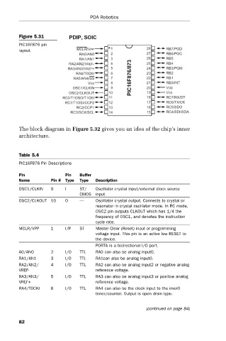
                          Figure 5.31
                          PIC16F876 pin              PDA Robotics
                          layout.


                          The block diagram in Figure 5.32 gives you an idea of the chip’s inner
                          architecture.


                          Table 5.4
                          PIC16F876 Pin Descriptions

                          Pin               Pin   Buffer
                          Name        Pin #  Type  Type  Description
                          OSC1/CLKIN  9     I    ST/   Oscillator crystal input/external clock source
                                                 CMOS  input.
                          OSC2/CLKOUT 10    O    —     Oscillator crystal output. Connects to crystal or
                                                       resonator in crystal oscillator mode. In RC mode,
                                                       OSC2 pin outputs CLKOUT which has 1/4 the
                                                       frequency of OSC1, and denotes the instruction
                                                       cycle rate.
                          MCLR/VPP    1     I/P  ST    Master Clear (Reset) input or programming
                                                       voltage input. This pin is an active low RESET to
                                                       the device.
                                                       PORTA is a bidirectional I/O port.
                          A0/AN0      2     I/O  TTL   RA0 can also be analog input0.
                          RA1/AN1     3     I/O  TTL   RA1can also be analog input0.
                          RA2/AN2/    4     I/O  TTL   RA2 can also be analog input2 or negative analog
                          VREF-                        reference voltage.
                          RA3/AN3/    5     I/O  TTL   RA3 can also be analog input3 or positive analog
                          VREF+                        reference voltage.
                          RA4/T0CKI   6     I/O  TTL   RA4 can also be the clock input to the imer0
                                                       timer/counter. Output is open drain type.


                                                                           (continued on page 84)

                          82
   101   102   103   104   105   106   107   108   109   110   111