
Page 112 - PDA Robotics Using Your Personal Digital Assistant to Control Your Robot
P. 112
PDA 05 5/30/03 11:35 AM Page 88
PDA Robotics
VDD
RBPU (2)
Weak
P Pull-up
Data Latch
Data Bus
D Q
I/O
WR Port (1)
CK pin
TRIS Latch
D Q
TTL
WR TRIS Input
CK Buffer
RD TRIS
Q D
RD Port
EN
RB0/INT
RB3/PGM
Schmitt Trigger RD Port
Buffer
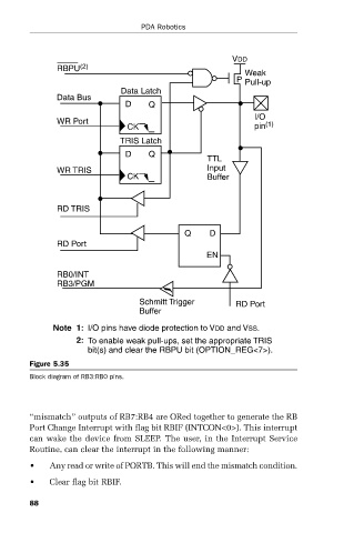
Note 1: I/O pins have diode protection to VDD and VSS.
2: To enable weak pull-ups, set the appropriate TRIS
bit(s) and clear the RBPU bit (OPTION_REG<7>).
Figure 5.35
Block diagram of RB3:RB0 pins.
“mismatch” outputs of RB7:RB4 are ORed together to generate the RB
Port Change Interrupt with flag bit RBIF (INTCON<0>). This interrupt
can wake the device from SLEEP. The user, in the Interrupt Service
Routine, can clear the interrupt in the following manner:
• Any read or write of PORTB. This will end the mismatch condition.
• Clear flag bit RBIF.
88