
Page 182 - Phase-Locked Loops Design, Simulation, and Applications
P. 182
DESIGN PROCEDURE FOR MIXED-SIGNAL PLLS Ronald E. Best 112
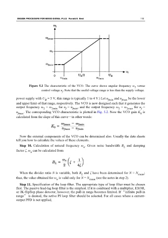
Figure 5.2 The characteristic of the VCO. The curve shows angular frequency ω versus
2
control voltage u . Note that the useful voltage range is less than the supply voltage.
f
power supply with U = 5 V, this range is typically 1 to 4 V.) Let u fmin and u fmax be the lower
B
and upper limit of that range, respectively. The VCO is now designed such that it generates the
output frequency ω = ω for u = u , and the output frequency ω = ω for u =
2 2min f fmin 2 2max f
u fmax . The corresponding VCO characteristic is plotted in Fig. 5.2. Now the VCO gain K is
0
calculated from the slope of this curve—in other words:
Now the external components of the VCO can be determined also. Usually the data sheets
tell you how to calculate the values of these elements.
Step 10. Calculation of natural frequency ω . Given noise bandwidth B and damping
L
n
factor ζ, ω can be calculated from
n
When the divider ratio N is variable, both B and ζ have been determined for N = N ;
L mean
thus, the value obtained for ω is valid only for N = N mean (see the notes in step 2).
n
Step 11. Specification of the loop filter. The appropriate type of loop filter must be chosen
first. The passive lead-lag loop filter is the simplest. If it is combined with a multiplier, EXOR,
or JK-flipflop phase detector, however, the pull-in range becomes limited. If “infinite pull-in
range” is desired, the active PI loop filter should be selected. For all cases where a current-
output PFD is not applied,