Page 253 - Phase-Locked Loops Design, Simulation, and Applications
P. 253
MIXED-SIGNAL PLL APPLICATIONS PART 1: INTEGER-N FREQUENCY
                SYNTHESIZERS   Ronald E. Best                                                          150
                 Noise model for resonant type VCOs. The situation is much better for resonant VCOs
               because we can use the noise model we already developed for the reference oscillator (see Sec.
               6.7.1). The final results have been given in Eqs. (6.11) through (6.14).
                 Contribution of VCO phase noise  to phase noise at PLL output. Knowing the noise
               models of both resonant and relaxation type VCOs, we can now compute the contribution of
               VCO phase noise to total phase noise at the output of the PLL. For this analysis, the noise
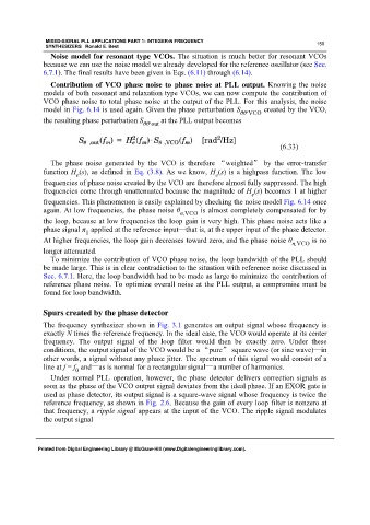
               model in Fig. 6.14 is used again. Given the phase perturbation S ,     created by the VCO,
                                                                              θθ VCO
               the resulting phase perturbation S ,   at the PLL output becomes
                                               θθ out


                                                                                           (6.33)


                 The phase noise generated  by the VCO is therefore  “weighted” by the error-transfer
               function H (s), as defined in Eq. (3.8). As we know, H (s) is a highpass function. The low
                          e                                           e
               frequencies of phase noise created by the VCO are therefore almost fully suppressed. The high
               frequencies come through unattenuated because the magnitude of H (s) becomes 1 at higher
                                                                                  e
               frequencies. This phenomenon is easily explained by checking the noise model Fig. 6.14 once
               again. At low frequencies, the phase noise θ n,VCO  is almost completely compensated for by

               the loop, because at low frequencies the loop gain is very high. This phase noise acts like a
               phase signal π  applied at the reference input—that is, at the upper input of the phase detector.
                             1
               At higher frequencies, the loop gain decreases toward zero, and the phase noise θ n,VCO  is no

               longer attenuated.
                 To minimize the contribution of VCO phase noise, the loop bandwidth of the PLL should
               be made large. This is in clear contradiction to the situation with reference noise discussed in
               Sec. 6.7.1. Here, the loop bandwidth had to be made as large to minimize the contribution of
               reference phase noise. To optimize overall noise at the PLL output, a compromise must be
               found for loop bandwidth.


               Spurs created by the phase detector
               The frequency synthesizer shown in Fig. 3.1 generates an output signal whose frequency is
               exactly N times the reference frequency. In the ideal case, the VCO would operate at its center
               frequency. The output signal of  the loop filter would then  be exactly zero. Under these
               conditions, the output signal of the VCO would be a “pure” square wave (or sine wave)—in
               other words, a signal without any phase jitter. The spectrum of this signal would consist of a
               line at f = f  and—as is normal for a rectangular signal—a number of harmonics.
                         0
                 Under normal PLL operation, however, the phase  detector delivers correction signals as
               soon as the phase of the VCO output signal deviates from the ideal phase. If an EXOR gate is
               used as phase detector, its output signal is a square-wave signal whose frequency is twice the
               reference frequency, as shown in Fig. 2.6. Because the gain of every loop filter is nonzero at
               that frequency, a ripple signal appears at the input of the VCO. The ripple signal modulates
               the output signal


             Printed from Digital Engineering Library @ McGraw-Hill (www.Digitalengineeringlibrary.com).

