
Page 258 - Phase-Locked Loops Design, Simulation, and Applications
P. 258
MIXED-SIGNAL PLL APPLICATIONS PART 1: INTEGER-N FREQUENCY
SYNTHESIZERS Ronald E. Best 153
We can eliminate the generation of subharmonic spurs by forcing the PFD to operate at a
nonzero phase error all the time. As shown in Fig. 6.21, a high-value resistor R slowly
3
discharges capacitor C toward ground. If the discharging current is higher than the charging
current produced by the parasitic capacitance, the PFD is forced to generate positive correction
pulses in every cycle of the reference signal. The ripple frequency is now identical with the
reference frequency. Because the cutoff frequency of the loop filter is lower than the reference
frequency in most cases, the ripple signal will be attenuated by the loop filter, which decreases
the level of the spurious sidebands. When resistor R is used, the spurious sidebands occur at
3
frequencies N · f ± f , N · f ± 2f , and so on.
ref ref ref ref
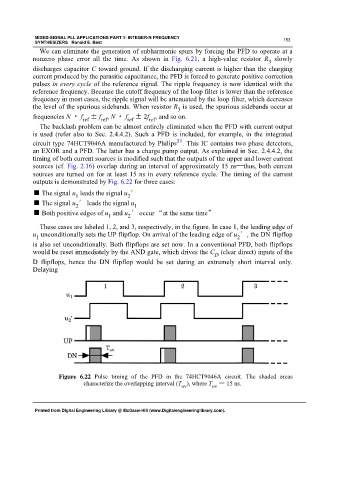
The backlash problem can be almost entirely eliminated when the PFD with current output
is used (refer also to Sec. 2.4.4.2). Such a PFD is included, for example, in the integrated
51
circuit type 74HCT9046A manufactured by Philips . This IC contains two phase detectors,
an EXOR and a PFD. The latter has a charge pump output. As explained in Sec. 2.4.4.2, the
timing of both current sources is modified such that the outputs of the upper and lower current
sources (cf. Fig. 2.16) overlap during an interval of approximately 15 ns—thus, both current
sources are turned on for at least 15 ns in every reference cycle. The timing of the current
outputs is demonstrated by Fig. 6.22 for three cases:
■ The signal u leads the signal u ′
1 2
■ The signal u ′ leads the signal u
2 1
■ Both positive edges of u and u ′ occur “at the same time”
1 2
These cases are labeled 1, 2, and 3, respectively, in the figure. In case 1, the leading edge of
u unconditionally sets the UP flipflop. On arrival of the leading edge of u ′, the DN flipflop
1
2
is also set unconditionally. Both flipflops are set now. In a conventional PFD, both flipflops
would be reset immediately by the AND gate, which drives the C (clear direct) inputs of the
D
D flipflops, hence the DN flipflop would be set during an extremely short interval only.
Delaying
Figure 6.22 Pulse timing of the PFD in the 74HCT9046A circuit. The shaded areas
characterize the overlapping interval (T ), where T ≈ 15 ns.
ov
ov
Printed from Digital Engineering Library @ McGraw-Hill (www.Digitalengineeringlibrary.com).