Page 260 - Phase-Locked Loops Design, Simulation, and Applications
P. 260
MIXED-SIGNAL PLL APPLICATIONS PART 1: INTEGER-N FREQUENCY
                SYNTHESIZERS   Ronald E. Best                                                          154
               the reset action by about 15 ns makes sure, however, that both flipflops remain in their
               “high” state for 15 ns after the leading edge of u ′. In case 2, where u ′ leads u , the
                                                                                                     1
                                                                  2
                                                                                          2
               leading edge of u ′ first sets the DN flipflop, and the UP flipflop is set later on the leading
                                2
               edge of u . Now a similar thing happens: delaying the reset of both flipflops by 15 ns lets both
                        1
               flipflops set for about 15 ns  after the leading edge of  u . Now assume that both positive
                                                                        1
               transients of u  and u ′ occur “at the same time.” Both flipflops are set immediately, and
                                    2
                             1
               they remain set for about 15 ns.
                 With this kind of PFD, there is a guaranteed overlap of both current outputs in every
               reference cycle. This virtually  inhibits the backlash effect  as described for voltage output
               PFDs. To demonstrate this, assume that the positive edge of u ′ is delayed by 1 ns against
                                                                            2
               the positive edge of u . In a conventional PFD, this time delay would fall below the backlash
                                    1
               interval, hence the PFD would not perform any reaction. In the case of the 74HCT9046A,
               however, the upper current source in Fig. 2.16c turns on the positive edge of u . One ns later,
                                                                                           1
               the positive edge of u ′ turns on the lower current source as well. From now on, both current
                                    2
               sources will be on for 15 ns. Consequently, the upper current source is on for 16 ns, and the
               lower for 15 ns. This results in a net positive charge supplied to the loop filter. If the u ′
                                                                                                       2
               signal would perform a positive transition 1 ns before the u signal, the lower current source
                                                                         1
               would be turned on first. The upper current source would then turn on 1 ns later. From this
               instant on, both current sources would remain on for 15 ns, hence the lower would conduct
               current for 16 ns, the upper for 15 ns, which would result in a net negative charge delivered to
               the loop filter. This demonstrates that even for the smallest time delay between the leading
               edges of  u  and  u ′, the PFD always feeds some charge into the loop filter. The pulse
                          1
                                  2
               widening due to parasitic capacitances (as shown in Fig. 6.21) does not play any role for this
               type of PFD because both current sources are turned on in  every reference cycle, thus
               canceling the widening effect.
                 There is nevertheless one source of error observed with charge pump PFDs: the imbalance
                                    53
               of the current sources  (cf. Fig. 2.16). When the source current does not exactly match the
               sink current and both current sources are ON during an identical interval of time, the charges
               do not compensate to zero but there is a nonzero charge delivered to the output of the PFD.
               When this happens, the PLL is forced to operate with nonzero phase error π . Consequently,
                                                                                          e
               the PFD must output a short output pulse in every reference cycle, and this leads to a spur at
               the reference frequency f .
                                       ref
                 To conclude, we give a couple of equations enabling us to estimate the spurs to be expected.
               Because the situation depends very much on the type of phase detector used, the equations are
               different for different phase detectors. Because the amplitude of the first pair of sidebands is
               always much greater than the amplitude of the higher ones, it is sufficient for practical
               purposes to have an approximation for the first sideband. In analogy to noise signals, sideband
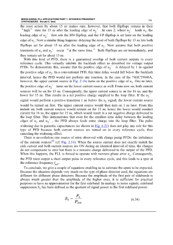
               suppression S  has been defined as the quotient of signal power to the first sideband power:
                            1


                                                                                           (6.34)

