
Page 128 - Photodetection and Measurement - Maximizing Performance in Optical Systems
P. 128
Useful Electronic Circuits and Construction Techniques to Get You Going
Useful Electronic Circuits and Construction Techniques to Get You Going 121
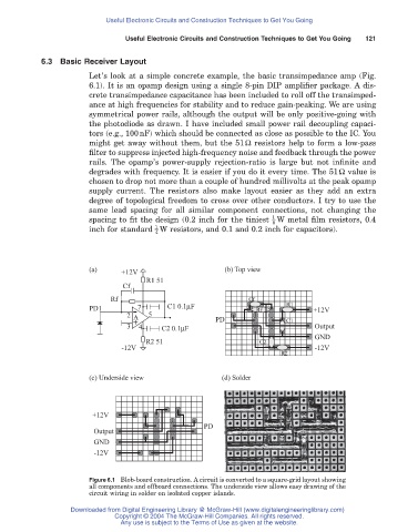
6.3 Basic Receiver Layout
Let’s look at a simple concrete example, the basic transimpedance amp (Fig.
6.1). It is an opamp design using a single 8-pin DIP amplifier package. A dis-
crete transimpedance capacitance has been included to roll off the transimped-
ance at high frequencies for stability and to reduce gain-peaking. We are using
symmetrical power rails, although the output will be only positive-going with
the photodiode as drawn. I have included small power rail decoupling capaci-
tors (e.g., 100nF) which should be connected as close as possible to the IC. You
might get away without them, but the 51W resistors help to form a low-pass
filter to suppress injected high-frequency noise and feedback through the power
rails. The opamp’s power-supply rejection-ratio is large but not infinite and
degrades with frequency. It is easier if you do it every time. The 51W value is
chosen to drop not more than a couple of hundred millivolts at the peak opamp
supply current. The resistors also make layout easier as they add an extra
degree of topological freedom to cross over other conductors. I try to use the
same lead spacing for all similar component connections, not changing the
1
spacing to fit the design (0.2 inch for the tiniest – W metal film resistors, 0.4
8
1
inch for standard – W resistors, and 0.1 and 0.2 inch for capacitors).
4
(a) +12V (b) Top view
R1 51
Cf
Rf Cf
PD1 - 7 C1 0.1μF Rf R1 +12V
2 + A 5 PD 1 C1
3 4 C2 0.1μF Output
GND
R2 51 C2
-12V -12V
R2
(c) Underside view (d) Solder
+12V
1
PD
Output
GND
-12V
Figure 6.1 Blob-board construction. A circuit is converted to a square-grid layout showing
all components and offboard connections. The underside view allows easy drawing of the
circuit wiring in solder on isolated copper islands.
Downloaded from Digital Engineering Library @ McGraw-Hill (www.digitalengineeringlibrary.com)
Copyright © 2004 The McGraw-Hill Companies. All rights reserved.
Any use is subject to the Terms of Use as given at the website.