
Page 30 - Photodetection and Measurement - Maximizing Performance in Optical Systems
P. 30
Amplified Detection Circuitry
Amplified Detection Circuitry 23
(a)
Photocurrent to
front-end receiver
+
-
Conducting layer
Guard
I Drive
V source
I PCB
Guard Guard
Protected
pin Photocurrent
(b)
I
V source
I PCB
Guard Guard
Insulator
Photocurrent
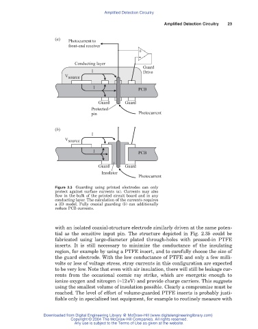
Figure 2.3 Guarding using printed electrodes can only
protect against surface currents (a). Currents may also
flow in the bulk of the printed circuit board and in any
conducting layer. The calculation of the currents requires
a 3D model. Fully coaxial guarding (b) can additionally
reduce PCB currents.
with an isolated coaxial-structure electrode similarly driven at the same poten-
tial as the sensitive input pin. The structure depicted in Fig. 2.3b could be
fabricated using large-diameter plated through-holes with pressed-in PTFE
inserts. It is still necessary to minimize the conductance of the insulating
region, for example by using a PTFE insert, and to carefully choose the size of
the guard electrode. With the low conductance of PTFE and only a few milli-
volts or less of voltage stress, stray currents in this configuration are expected
to be very low. Note that even with air insulation, there will still be leakage cur-
rents from the occasional cosmic ray strike, which are energetic enough to
ionize oxygen and nitrogen (ª12eV) and provide charge carriers. This suggests
using the smallest volume of insulation possible. Clearly a compromize must be
reached. The level of effort of volume-guarded PTFE inserts is probably justi-
fiable only in specialized test equipment, for example to routinely measure with
Downloaded from Digital Engineering Library @ McGraw-Hill (www.digitalengineeringlibrary.com)
Copyright © 2004 The McGraw-Hill Companies. All rights reserved.
Any use is subject to the Terms of Use as given at the website.