
Page 28 - Photodetection and Measurement - Maximizing Performance in Optical Systems
P. 28
Amplified Detection Circuitry
Amplified Detection Circuitry 21
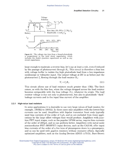
Voltage
Follower
I p
+ A V o = I R
p L
C p R L -
V Rise time (10–90%): 2.2 R C
b L p
p
Battery Bandwidth: 1/2 R C
L p
I p
63% 86% 95% 98%
V o
0 1RC 2RC 3RC 4RC
Time (s)
Figure 2.2 The voltage rise time from a biased photodiode
is proportional to the total shunt capacitance, which
includes the diode’s junction capacitance as well as any
circuit capacitance.
large enough to maintain a reverse bias, let’s say at least a volt, even if reduced
by the passage of photocurrent through R L. This circuit is therefore a bias box
with voltage buffer to isolate the high photodiode load from a low-impedance
oscilloscope or voltmeter input. The output voltage at DC is as before just the
photocurrent I p flowing through the load resistor R L :
V o = I R L . (2.1)
p
This circuit allows use of load resistors much greater than 1MW. The limit
comes, as with the bias box, when the voltage dropped across the load resistor
becomes comparable with the bias voltage (V b), whatever its origin. The load
resistor voltage is due not only to photocurrent, but also to photodiode “dark”
leakage currents and to the input bias current of the amplifier.
2.3.1 High-value load resistors
In some applications it is desirable to use very large values of load resistor, for
example, 100MW to 100GW. In these cases only amplifiers with the lowest bias
currents can be used. Amplifiers with bipolar transistor front ends typically
need bias currents of the order of 1mA, and so are excluded from these appli-
cations by the large offset voltages they would produce. Amplifiers with junc-
tion FET input stages, such as the popular LF356 series, require bias currents
of the order of 200pA, and so can perform better. Amplifiers with metal oxide
semiconductor FET (MOSFET) input devices, such as the CA3140, offer input
bias currents of the order of a few tens of picoamperes down to a picoampere,
and so can be used with gigohm resistors without excessive offsets. Specially
optimized amplifiers, such as the Analog Devices AD515 (±75fA), Burr-Brown
Downloaded from Digital Engineering Library @ McGraw-Hill (www.digitalengineeringlibrary.com)
Copyright © 2004 The McGraw-Hill Companies. All rights reserved.
Any use is subject to the Terms of Use as given at the website.