
Page 24 - Photodetection and Measurement - Maximizing Performance in Optical Systems
P. 24
Photodetection Basics
Photodetection Basics 17
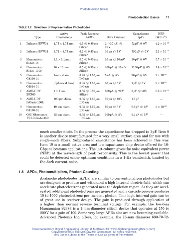
TABLE 1.2 Selection of Representative Photodiodes
Active Peak Respons. Capacitance NEP
Type Dimensions (A/W) Dark Current (pF) (W/Hz )
1 / 2
1 Infineon BPW34 2.75 ¥ 2.75mm 0.6 @ 0.85mm 2 (<30nA) @ 72pF @ 0V 4.2 ¥ 10 -14
Silicon 10V
2 Infineon BPW33 2.75 ¥ 2.75mm 0.6 @ 0.85mm 20pA @ 1V 750pF @ 0V 5.3 ¥ 10 -15
Silicon
3 Hamamatsu 1.1 ¥ 1.1mm 0.5 @ 0.95mm 20pA @ 10mV 20pF @ 0V 5.7 ¥ 10 -15
S1336-18 Silicon
4 Hamamatsu 10 ¥ 10mm 0.5 @ 0.95mm 200pA @ 10mV 1100pF @ 0V 1.8 ¥ 10 -14
S1337-1010 Silicon
5 Hamamatsu 1-mm diam. 0.95 @ 1.55mm 5nA @ 5V 90pF @ 5V 2 ¥ 10 -14
G8370-01 InGaAs
6 Hamamatsu (Spherical lens) 0.95 @ 1.55mm 80pA @ 5V 1pF @ 5V 2 ¥ 10 -15
G6854-01 InGaAs
7 AME-UDT 1 ¥ 1mm 0.55 @ 0.90mm 500pA @ 20V 3pF @ 20V 2.3 ¥ 10 -14
BPX65 Silicon
8 AME-UDT 100-mm diam. 0.95 @ 1.55mm 50pA @ 10V 1.5pF —
InGaAs-100L InGaAs
9 Hamamatsu 40-mm diam. 0.95 @ 1.55mm 60pA @ 5V 0.6pF @ 2V 2 ¥ 10 -14
G8198-01 InGaAs
10 OSI Fibercomm 25-mm diam. 0.95 @ 1.55mm 100pA @ 5V 0.2pF @ 5V —
FCI-InGaAs-25C InGaAs
much smaller diode. In the process the capacitance has dropped to 1pF. Item 9
is another device manufactured for a very small surface area and for use with
single-mode fibers. Subpicofarad capacitance has been achieved in this way.
Item 10 is a small active area and low capacitance chip device offered for 10-
Gbps telecomms applications. The last column gives the noise equivalent power
(NEP) at the wavelength of peak responsivity. This is the lowest power that
could be detected under optimum conditions in a 1-Hz bandwidth, limited by
the dark current noise.
1.8 APDs, Photomultipliers, Photon-Counting
Avalanche photodiodes (APDs) are similar to conventional pin photodiodes but
are designed to produce and withstand a high internal electric field, which can
accelerate photoelectrons generated near the depletion region. As they are accel-
erated, additional photoelectrons are generated and a cascade process produces
10 to 1000 photoelectrons per incident photon. This high internal gain can be
of great use in receiver design. The gain is produced through application of
a higher than normal reverse terminal voltage. For example, the low-bias
Hamamatsu S2383 is a 1-mm-diameter silicon device that operates at 150 to
200V for a gain of 100. Some very large APDs also are now becoming available.
Advanced Photonix Inc. offers, for example, the 16-mm diameter 630-70-72-
Downloaded from Digital Engineering Library @ McGraw-Hill (www.digitalengineeringlibrary.com)
Copyright © 2004 The McGraw-Hill Companies. All rights reserved.
Any use is subject to the Terms of Use as given at the website.