Page 119 - Photonics Essentials an introduction with experiments
P. 119
Light-Emitting Diodes

                                                    Light-Emitting Diodes  113

            The external efficiency of the LED, which is based on the actual
          light that gets emitted, can be optimized by placing the light emission
          region close to the physical surface. The minority carrier injection effi-
          ciency for electrons, which we will call
 e in order to distinguish it
          from the quantum efficiency, is given in Eq 6.9.

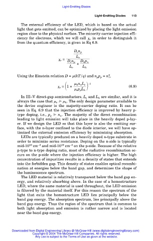
                                         D e n p

                                          L e

 e =
                                     D e n p  D h p n
                                        +
                                       L e    L h
          Using the Einstein relation D =  (kT/q) and n p p p = n i ,
                                                            2
                                           h n n L e   –1

 e = 1 +                              (6.9)
                                           e p p L h
            In III–V direct-gap semiconductors, L e and L h are similar, and it is
          always the case that   e     h . The only design parameter available to
          the device engineer is the majority-carrier doping ratio. It can be
          seen in Eq. 6.9 that the injection efficiency is improved by heavy p-
          type doping, i.e., p p   n n . The majority of the direct recombination
          leading to light emission will take place in the heavily doped p-lay-
          er. If we design the LED so that this layer is also the emitting sur-
          face, with the n-layer confined to the diode interior, we will have op-
          timized the external emission efficiency by minimizing absorption.
            LEDs are typically produced on a heavily doped n-type substrate in
          order to minimize series resistance. Doping on the n-side is typically
          mid-10 16  cm –3  and mid-10 19  cm –3  on the p-side. Because of the relative
          p-type to n-type doping ratio, most of the radiative recombination oc-
          curs on the p-side where the injection efficiency is higher. The high
          concentration of impurities results in a density of states that extends
          into the forbidden gap. This density of states enables optical recombi-
          nation at energies below the band gap, and determines the shape of
          the luminescence spectrum.
            The LED material is relatively transparent below the band gap en-
          ergy, and relatively absorbing above. In the case of a homostructure
          LED, where the same material is used throughout, the LED emission
          is filtered by the material itself. For this reason the spectrum of the
          light that exits the homostructure LED lies principally below the
          band gap energy. The absorption spectrum, lies principally above the
          band gap energy. Thus the region of the spectrum that is common to
          both light absorption and emission is rather narrow and is located
          near the band gap energy.


       Downloaded from Digital Engineering Library @ McGraw-Hill (www.digitalengineeringlibrary.com)
                   Copyright © 2004 The McGraw-Hill Companies. All rights reserved.
                    Any use is subject to the Terms of Use as given at the website.

