
Page 151 - Photonics Essentials an introduction with experiments
P. 151
Lasers
Lasers 145
its resistance to common between the output and common is very high
compared to the 10 kW resistor in the collector circuit. The voltage at
the output relative to common is very close to the bias voltage of 5 V.
On the other hand, if the bias on the gate is raised so it is close to 5 V,
the transistor will turn on and its resistance will now be low com-
pared to 10 kW. So the voltage at the output will be close to common
or 0 V. The output voltage is thus essentially the opposite of the input
voltage. In fact, if we vary the input voltage sinusoidally between 0
and 5 V, the output voltage will also vary sinusoidally between 0 and
5 V, but 180° out of phase with the input. The input current that ac-
companies the input voltage is smaller than the output current, so
there is amplification given by the ratio of the output current to the
input current.
In the next step, we would like to introduce some feedback from the
output to the input in order to see what happens.
The simplest feedback element is a direct connection between the
output and the input. Since the output is essentially 180° out of phase
with the input, the effect of the feedback on the small-signal gain will
be to oppose any changes in the input at the base. This is a negative
feedback circuit. The result will be that the transistor will operate in
a stable state that is midway between being totally on and totally off,
+
with the output pegged at V /2. More moderate degrees of negative
feedback can be achieved by putting resistance in the feedback circuit.
This approach is commonly used to stabilize the amplifier, and to im-
prove its frequency bandwidth at the expense of peak gain.
Now suppose that the goal is not to obtain a wide amplifier band-
width, but rather the opposite extreme: that is, an amplifier with all
the gain peaked around one frequency. This could be achieved by ap-
plying positive feedback from the output to the input. The result is a
circuit that amplifies only one frequency. This is a way to define an
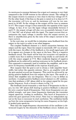
oscillator. A simple positive feedback circuit element is a RC combina-
tion that produces a 180° phase shift in the output signal for the par-
ticular frequency. Such a circuit is shown in Fig. 7.2.
The feedback circuit transmits a wide band of frequencies to the in-
put, but the 180° phase shift leading to positive feedback is obtained
for only a narrow band of frequencies. Only these frequencies are am-
plified strongly, and soon these frequencies dominate the transistor
output spectrum, leading to oscillation. This band of frequencies is
called the gain spectrum of the circuit. Note that no independent sig-
nal on the base is necessary to start oscillation. The oscillation builds
up from the noise components having the same frequency as the high-
ly peaked gain spectrum.
Note that the single-frequency characteristic of the oscillator is de-
termined largely by the elements of the feedback circuit. Indeed, you
Downloaded from Digital Engineering Library @ McGraw-Hill (www.digitalengineeringlibrary.com)
Copyright © 2004 The McGraw-Hill Companies. All rights reserved.
Any use is subject to the Terms of Use as given at the website.