
Page 406 - Power Electronic Control in Electrical Systems
P. 406
//SYS21/F:/PEC/REVISES_10-11-01/075065126-CH009.3D ± 385 ± [373±406/34] 17.11.2001 10:33AM
Power electronic control in electrical systems 385
conditions. The series inductive reactance of the line is X L 48:0
and the
shunt capacitive susceptance is B c 4000 mS. Calculate
(i) the transmission angle d when the load is 1540 MW;
(ii) the value of the compensating susceptance B g and reactance X g at this load.
2E 2 d 2 500 2 d
(i) P sin 1540 sin
X L 2 48 2
so d 17:0 .
B c 4 E d
(ii) B g 1 cos
2 X L E m 2
4000 10 6 4 17
1 cos 0:00108 S
2 48 2
so X g 1/0:00108 922
.
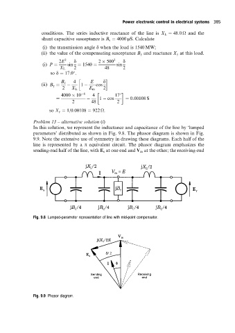
Problem 13 ± alternative solution (i)
In this solution, we represent the inductance and capacitance of the line by `lumped
parameters'distributed as shown in Fig. 9.8. The phasor diagram is shown in Fig.
9.9. Note the extensive use of symmetry in drawing these diagrams. Each half of the
line is represented by a p equivalent circuit. The phasor diagram emphasizes the
sending-end half of the line, with E s at one end and V m at the other; the receiving-end
Fig. 9.8 Lumped-parameter representation of line with mid-point compensator.
Fig. 9.9 Phasor diagram.