
Page 102 - Power Electronics Handbook
P. 102
Smartpower 95
(b) E> Body
Leads
(c) Leads
Chip
Ceramic cover
Metal lead frame
(4
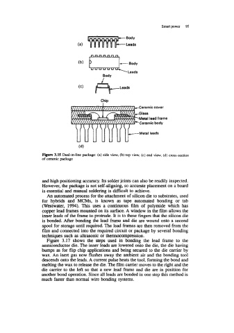
Figure 3.15 Dual-in-line package: (a) side view, (b) top view, (c) end view, (d) cross-section
of ceramic package
and high positioning accuracy. Its solder joints can also be readily inspected.
However, the package is not self-aligning, so accurate placement on a board
is essential and manual soldering is difficult to achieve.
An automated process for the attachment of silicon die to substrates, used
for hybrids and MCMs, is known as tape automated bonding or tab
(Westwater, 1994). This uses a continuous film of polymide which has
copper lead frames mounted on its surface. A window in the film allows the
inner leads of the frame to protrude. It is to these fingers that the silicon die
is bonded. After bonding the lead frame and die are wound onto a second
spool for storage until required. The lead frames are then removed from the
film and connected into the required circuit or package by several bonding
techniques such as ultrasonic or thennocompression.
Figure 3.17 shows the steps used in bonding the lead frame to the
semiconductor die. The inner leads are lowered onto the die, the die having
bumps as for flip chip applications and being secured to the die carrier by
wax. An inert gas now flushes away the ambient air and the bonding tool
descends onto the leads. A current pulse heats the tool, forming the bond and
melting the wax to release the die. The film carrier moves to the right and the
die carrier to the left so that a new lead frame and die are in position for
another bond operation. Since all leads are bonded in one step this method is
much faster than normal wire bonding systems.