
Page 90 - Power Electronics Handbook
P. 90
Isolating components 83
maximum voltage which can be applied between input and output without
breakdown. If breakdown occurs it can form a resistive path due to
carbonised moulding on the surface, or it can result in a short circuit caused
by molten lead wires bridging the lead frames of the emitter and detector.
For high isolation voltages the moulding is usually designed such that the
input and output pins are brought out from separate sides of the package.
It is also important to minimise the parasitic capacitance through the
dielectric between input and output.
The current transfer ratio is given as the ratio of the output current to the
input current of the source, when the detector is biased in a specified way.
This ratio is determined by several factors, such as the level of current into
the source and detector saturation. Generally, an LED is used as a source
and the light output of the device falls with time, giving a decrease of
transfer ratio. The operating speed of the coupler defines how fast it can be
switched and is usually specified in terms of its maximum operating
frequency.
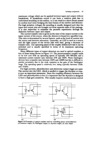
Many different types of output detectors are used in optical couplers, a
few of these being shown in Figure 3.9. The phototransistor coupler tends
to’ be low cost with an operating speed of typically 1OO-u)okHz and a
minimum current transfer ratio between 20% and 300%. Photo Darlington
devices have a transfer ratio between 100% and 1OOO% but this is difficult to
predict accurately due to the wide variation in the gain of the Darlington
stage. The operating speed is relatively low, being typically between 2kHz
and 1OkHz.
For high currents, photothyristor and phototriac output stages are used.
The current into the LED, which is needed to trigger the thyristor or triac,
is now an important parameter. Since the coupling efficiency between the
LED and photothyristor is low it is important that the thyristor is designed
to have a high gate sensitivity. This usually requires careful process control
r---------t
L ________
J
(C) (d)
Figure 3.9 Examples of optical couplers used for controlling power semiconductors:
(a) transistor output; (b) Darlington output; (c) thyristor output; (d) triac output