
Page 86 - Power Electronics Handbook
P. 86
Trigger devices 79
ov
(e)
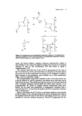
Firprr 3.4 Complementary and programmable unijunction transistors: (a) complementary
unijuaction transistor (CVJT); (b) CUJTsymbol; (c) programmable unijunction transistor
(PUT); (d) PUT symbol; (e) a PUT oscillator circuit
mode, the device exhibits a negative resistance characteristic, similar to
that of Figure 3.3(e). Since the applied voltages and currents are of polarity
opposite to that of the conventional UJT this device is called a
complementary UJT.
The intrinsic stand-off ratio of the CUJT is determined by the ratio of
the two resistors R1 and R2 and since these are situated on the same silicon
die as the rest of the components the device can be designed to exhibit a
tight tolerance in this parameter, good stability over a wide temperature
range, and low saturation voltage.
The programmable unijunction transistor is also a four-layer device but
it has its resistors R1 and R2 external to the silicon die so that they can be
selected by the user. This enables parameters such as the intrinsic stand-off
ratio, interbase resistance and the peak and valley point currents, to be
programmable. By choice of suitable external components these para-
meters can be made less susceptible to temperature variations than a
conventional UJT. As seen from its symbol, the PUT is basically a thyristor
with an anode gate.
Figure 3.4(e) shows the PUT used in a relaxation oscillator circuit similar
to that of Figure 3.3(f). External resistors R1 and R2 determine the value of
the intrinsic stand-off ratio for the device and timing circuit R5C1 can be
modified to vary the oscillator frequency. Diode D1 compensates for the