
Page 82 - Power Electronics Handbook
P. 82
Trigger devices 75
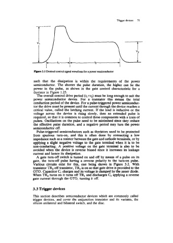
3.1 Desired control signal waveform for a power semiconductor
such that the dissipation is within the requirements of the power
semiconductor. The shorter the pulse duration, the higher can be the
power in the pulse, as shown in the gate control characteristic for a
thyristor in Figure 1.25.
The overall control drive period (rl+r2) must be long enough to suit the
power semiconductor device. For a transistor this means the total
conduction period of the device. For a pulse-triggered power semiconduc-
tor the drive must be present until the current through the device reaches a
critical value, called the latching current. If the load is inductive or the
voltage across the device is rising slowly, then an extended pulse is
required, so that it is common to control these components with a train of
pulses. Oscillations on the pulse need to be minimised since they reduce
the effective pulse duration, and a negative period may turn the power
semiconductor off.
Pulse-triggered semiconductors such as thyristors need to be protected
from spurious turn-on, and this is often done by conneding a low
impedance such as a resistor between the gate and cathode terminals, or by
applying a slight negative voltage to the gate terminal when it is to be
non-conducting. A positive voltage on the gate terminal is also to be
avoided when the device is reverse biased since it increases its leakage
current and hence its dissipation.
A gate turnsff switch is turned on and off by means of a pulse on its
gate, the turn-off pulse having a reverse polarity to the turn-on pulse.
Various circuits exist for this, one being shown in Figure 3.2. With
transistor TR2 off transistor, TR1 is on so that gate drive is provided to the
GTO. Capacitor C1 charges and its voltage is clamped by the zener diode.
When TR2 turns on it turns off TR1 and discharges C1 applying a reverse
gate current through the GTO, turning it off.
3.3 Trigger devices
This section describes semiconductor devices which are commonly called
trigger devices, and cover the unijunction transistor and its variants, the
silicon unilateral and bilateral switch, and the diac.