
Page 83 - Power Electronics Handbook
P. 83
76 Power semiconductor control components
+vs
7 GTO
v
Onloff
ov
control
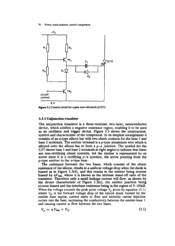
3.2 Coatrol Circuit for a gate turn-off switch (GTO)
3.3.1 U~unction transistor
The unijunction transistor is a three-terminal, two-layer, semiconductor
device, which exhibits a negative resistance region, enabling it to be used
as an oscillator and trigger device. Figure 3.3 shows the construction,
symbol and characteristic of the component. In its simplest arrangement it
consists of an n-type silicon bar with two ohmic contacts for the base 1 and
base 2 terminals. The emitter terminal is a p-type aluminium wire which is
alloyed onto the silicon bar to form a p-n junction. The symbol for the
UJT shows base 1 and base 2 terminals at right angles to indicate that these
are non-rectifying ohmic contacts, but the emitter is represented by an
arrow since it is a rectifying p-n junction, the arrow pointing from the
p-type emitter to the n-type base.
The resistance between the two bases, which consists of the ohmic
resistance of the silicon, results in a uniform voltage drop when the diode is
biased as in Figure 3.3(d), and this results in the emitter being reverse
biased by qVBB, where q is known as the intrinsic stand-off ratio of the
transistor. Therefore only a small leakage current will flow, as shown by
the device characteristic of Figure 3.3(e), the emitter junction being
reverse biased and the interbase resistance being in the region of 5-10 kQ.
When the voltage exceeds the peak point voltage Vp given by equation (3.1)
where V,, is the forward voltage drop of the silicon diode formed by the
emitter base region, current starts to flow and minority carrier injection
occurs into the base, increasing the conductivity between the emitter-base 1
and causing current to flow between the two bases.
vp = VBB + VD (3.1)