
Page 85 - Power Electronics Handbook
P. 85
78 Power semiconductor control components
device is in its saturation region most of the power dissipation occurs in the
emitter-base 2 resistance, which can result in localised heating; it can be
minimised by use of a suitable external resistance in the base 2 lead, as
shown in Figure 3.30.
The peak and valley point currents and voltages are also given in data
sheets and these define the negative resistance region. The valley point
location is affected by the temperature and the value of the interbase
voltage, whilst the peak point is a function of this voltage and the intrinsic
stand-off ratio. The emitter-base 2 leakage current, when this junction is
reverse biased with base 1 open, is also given in the data sheets. It is similar
in value to that of leakage through a diode, and it affects the charging
current of any capacitors used in timing circuits, so that it needs to be taken
into account in the circuit design. The intrinsic stand-off ratio, given in data
sheets, is a very important parameter in the design of UJT circuits, and
although it varies from one UJT to another, it remains relatively constant
for a device even with variations in supply voltage and temperature.
Figures 3.3(b) and 3.3(c) show two other structures used for unijunction
transistors. The cube arrangement gives a smaller distance between the
emitter and base 1 and therefore has a smaller active area, giving faster
turn-on times. The planar structure allows lengths to be accurately
controlled, which results in shorter distances between emitter and base 1
and a smaller chip size. This again results in faster turn-on times. The peak
point current, valley point current and emitter saturation voltage are also
decreased and so the device gives good sensitivity and low trigger currents,
which is useful for long time-delay circuits since large-valued timing
resistors can now be used, and capacitor sizes can be reduced. However,
the average emitter current, which is often the load current, is also reduced
so that the drive output is lower, requiring amplification before it can be
used to control power semiconductors.
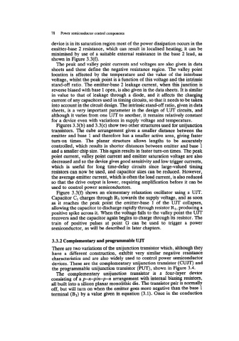
Figure 3.3(f) shows an elementary relaxation oscillator using a UJT.
Capacitor CI charges through R3 towards the supply voltage, and as soon
as it reaches the peak point the emitter-base 1 of the UJT collapses,
allowing the capacitor to discharge rapidly through resistor R1, producing a
positive spike across it. When the voltage falls to the valley point the UJT
recovers and the capacitor again begins to charge through its resistor. The
train of positive pulses at point G can be used to trigger a power
semiconductor, as will be described in later chapters.
3.3.2 Complementary and programmable UJT
There are two variations of the unijunction transistor which, although they
have a different construction, exhibit very similar negative resistance
characteristics and are also widely used to control power semiconductor
devices. These are the complementary unijunction transistor (CUJT) and
the programmable unijunction transistor (PUT), shown in Figure 3.4.
The complementary unijunction transistor is a four-layer device
consisting of a p-n-pln-p-n arrangement with internal biasing resistors,
all built into a silicon planar monolithic die. The transistor pair is normally
off, but will turn on when the emitter goes more negative than the base 1
terminal (B1) by a value given in equation (3.1). Once in the conduction