
Page 51 - Principles and Applications of NanoMEMS Physics
P. 51
1. NANOELECTROMECHANICAL SYSTEMS 37
(
three main modalities, namely, single-walled nanotubes SWNTs), which
range in diameter from approximately 0.4nm to more than 3nm, multi-
walled nanotubes (MWNTs), which range in diameter from approximately
1.4nm to more than 100nm, and ropes, which are parallel stripes of SWNTs
stuck to each other. Their physical properties are astounding. With aspect
µ
ratios of the order of 10-1000, they are several m (ropes up to cm) long,
possess a Young’s modulus, tensile strength, and density of ~1TPa (Steel:
3
g
0.2TPa), 45GPa (Steel: 2 GPa), and 1.33 ~ 1.4 / cmg 3 (Al: 2.7 / cm ). In
addition, their conductivity may be metallic or semiconducting, and they
3
3
have a current carrying capability of ~1TA / cm (Cu: 1GA / cm ). A
number of techniques are employed to produce CNTs, for instance, the arc
discharge, laser ablation and chemical vapor deposition methods. These
methods usually yield a random mixture of SWNTs, MWNTs, and ropes and
research is under way to determine techniques for the controlled growth of a
specific type of CNT. For instance, Li et al. [47] have reported the
development of a catalyst-based method that predominantly yields SWNT.
In this method, a silicon wafer is pre-patterned with alumina nanoparticles,
which serve as catalysts for their CVD growth, producing SWNTs with
diameter under 1.5nm.
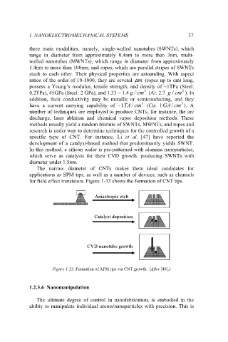
The narrow diameter of CNTs makes them ideal candidates for
applications as SPM tips, as well as a number of devices, such as channels
for field effect transistors. Figure 1-33 shows the formation of CNT tips.
Anisotropic etch
Anisotropic etch
Catalyst deposition
Catalyst deposition
CVD nanotube growth
CVD nanotube growth
Figure 1-33. Formation of AFM tips via CNT growth. (After [48].)
1.2.3.6 Nanomanipulation
The ultimate degree of control in nanofabrication, is embodied in the
ability to manipulate individual atoms/nanoparticles with precision. This is