
Page 196 - Programming Microcontrollers in C
P. 196
Timers 181
tive to the internal 16-bit counter. This value is placed into an output
compare register. The content of the counter is compared automati
cally by the microcontroller to the value in the output compare register
at each count of the counter. When the two values are equal, a flag is
set, an output occurs, and if desired, the CPU is interrupted. The
output compare system can be used to generate waveforms, to con
trol phases between different waveforms, to control events based on
calculated times.
Different microcontrollers will have differing numbers of input
capture and output compare registers. In the discussions that follow,
details of a single input capture and output compare register will be
discussed. It is assumed that these registers are part of an
M68HC05B6, so there are two input captures and two output com
pares onthe microcontroller. For details on access to the second
register set, refer to the appropriate data manual. Later we will see
microcontrollers that have many more input capture and output com
pare systems (up to 16 on one microcontroller).
Timer Control Register
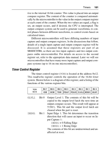
The timer control register (TCR) is located at the address 0x12.
This read/write register controls the operation of the 16-bit timer
system. Shown below is a diagram of this register, and a listing of the
functions of the various register bits.
TCR Bit 7 Bit 6 Bit 5 Bit 4 Bit 3 Bit 2 Bit 1 Bit 0
0x12 ICIE OCIE TOIE FOLV1 FOLV2 CLVL2 IEDG1 OLVI1
OLVL1 Bit 0 Output Level 1. The contents of this bit will be
copied to the output level latch the next time an
output compare occurs. This result will appear at
TCMP1. This bit and the output level latch are
cleared when the part is reset.
IEDG1 Bit 1 Input Edge 1. This bit determines the transition
direction that will cause an input to occur on In
put Capture 1:
IEDG1 = 0 Falling Edge
IEDG1 = 1 Rising Edge
The contents of this bit are undetermined and un
affected at reset.