
Page 216 - Radiochemistry and nuclear chemistry
P. 216
200 Radiochemistry and Nuclear Chemistry
o VO vp/v0
1.0
Re
0.9
Ce
A
0.8
II
0.?
T C, I I I I l I
0.6
I 2 3 4 5 6
t(iJs)
(a) (b)
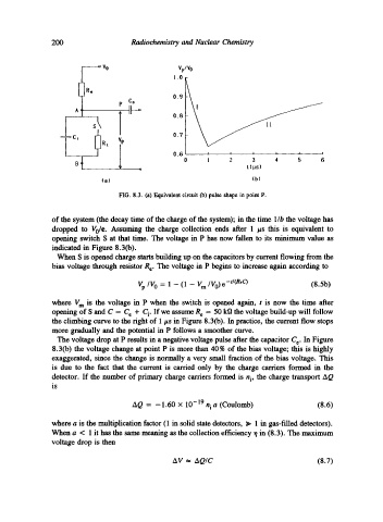
FIG. 8.3. (a) Equivalent circuit (b) pulse shape in point P.
of the system (the decay time of the charge of the system); in the time 1/b the voltage has
dropped to Vole. Assuming the charge collection ends after 1 /~s this is equivalent to
opening switch S at that time. The voltage in P has now fallen to its minimum value as
indicated in Figure 8.3(b).
When S is opened charge starts building up on the capacitors by current flowing from the
bias voltage through resistor R e. The voltage in P begins to increase again according to
Vp IV o = 1 - (1 - V m/Vo) e -*/(R'O (8.5b)
where V m is the voltage in P when the switch is opened again, t is now the time after
opening of S and C = C e + C i. If we assume R e = 50 k9 the voltage build-up will follow
the climbing curve to the fight of 1/zs in Figure 8.3(b). In practice, the current flow stops
more gradually and the potential in P follows a smoother curve.
The voltage drop at P results in a negative voltage pulse after the capacitor C e. In Figure
8.3(b) the voltage change at point P is more than 40% of the bias voltage; this is highly
exaggerated, since the change is normally a very small fraction of the bias voltage. This
is due to the fact that the current is carried only by the charge carriers formed in the
detector. If the number of primary charge carriers formed is n i, the charge transport AQ
is
AQ = -1.60 • 10 -19 n i a (Coulomb) (8.6)
where a is the multiplication factor (1 in solid state detectors, ~ 1 in gas-fillext detectors).
When a < 1 it has the same meaning as the collection efficiency ~/in (8.3). The maximum
voltage drop is then
AV .~ AQ/C (8.7)