
Page 228 - Radiochemistry and nuclear chemistry
P. 228
212 Radiochemistry and Nuclear Chemistry
I
~176 I m .R ~11 iool. Ioo. - I.o . §
oo
oo
|
oo
o@
o
oo
p
n
P n oo@ n o p Q
.J --I
_<
Z
k-
O
Q.
DISTANCE DISTANCE
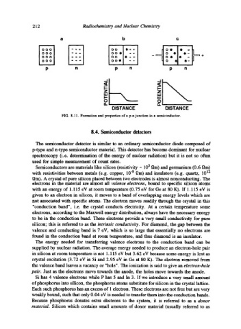
FIG. 8.11. Formation and properties of a p-n junction in a semiconductor.
8.4. Semiconductor detectors
The semiconductor detector is similar to an ordinary semiconductor diode composed of
p-type and n-type semiconductor material. This detector has become dominant for nuclear
spectroscopy (i.e. determination of the energy of nuclear radiation) but it is not so often
used for simple measurement of count rates.
Semiconductors are materials like silicon (resistivity ~ 10 3 l~m) and germanium (0.6 Ore)
with resistivities between metals (e.g. copper, 10 "8 0m) and insulators (e.g. quartz, 1012
rim). A crystal of pure silicon placed between two electrodes is almost nonconducting. The
electrons in the material are almost all valence electrons, bound to specific silicon atoms
with an energy of 1.115 eV at room temperature (0.75 eV for Ge at 80 K). If 1.115 eV is
given to an electron in silicon, it moves to a band of overlapping energy levels which are
not associated with specific atoms. The electron moves readily through the crystal in this
"conduction band", i.e. the crystal conducts electricity. At a certain temperature some
electrons, according to the Maxwell energy distribution, always have the necessary energy
to be in the conduction band. These electrons provide a very small conductivity for pure
silicon; this is referred to as the intrinsic conductivity. For diamond, the gap between the
valence and conducting band is 7 eV, which is so large that essentially no electrons are
found in the conduction band at room temperature, and thus diamond is an insulator.
The energy needed for transferring valence electrons to the conduction band can be
supplied by nuclear radiation. The average energy needed to produce an electron-hole pair
in silicon at room temperature is not 1.115 eV but 3.62 eV because some energy is lost as
crystal excitation (3.72 eV in Si and 2.95 eV in Ge at 80 K). The electron removed from
the valence band leaves a vacancy or "hole'. The ionization is said to give an electron-hole
pair. Just as the electrons move towards the anode, the holes move towards the anode.
Si has 4 valence electrons while P has 5 and In 3. If we introduce a very small amount
of phosphorus into silicon, the phosphorus atoms substitute for silicon in the crystal lattice.
Each such phosphorus has an excess of 1 electron. These electrons are not free but are very
weakly bound, such that only 0.04 eV is needed to transfer them into the conduction bands.
Because phosphorus donates extra electrons to the system, it is referred to as a donor
material. Silicon which contains small amounts of donor material (usually referred to as