
Page 230 - Radiochemistry and nuclear chemistry
P. 230
214 Radiochemistry and Nuclear Chemistry
8.4.1. Surface barrier detectors
The surface barrier detector is a p-n type silicon diode wafer characterized by a rather
thin depletion layer (Fig. 8.12(a)). It is made of n-type silicon on which one surface has
been etched prior to coating with a thin layer of gold (typically -40 #g/era 2) and the other
surface coated with a thin layer of aluminum (typically -40 ttg/cm 2) to provide electrical
contact. This results in a window-layer which is equivalent to --800 A, of Si. Depending on
the applied voltage, the detector can be partially depleted (inactive entrance layer), totally
depleted (no inactive layer), or overdepleted (higher applied potential than required for total
depletion). Surface barrier detectors are used mainly for a- and/3-spectroscopy and for
dE/dx and E measurements for high energy particles, although the efficiency is limited by
the sensitive surface diameter ( < 10 era) and the energy range by depleted layer thickness
(< 5ram).
The radiation sensitive depleted layer is available in various thicknesses, _< 5 ram, enough
to stop electrons of < 2.2 MeV, p of < 32 MeV, and ot of < 120 MeV. A typical silicon
surface barrier detector for t~-spectroscopy has a sensitive area of 300 mm 2, 300 #m
depletion depth, 20 keV FWHM (full width at half maximum) and operates at 100 V
reverse bias. The resolving time is about 10 -8 s. Special "rugged" detectors are available
which have an acid resistant SiO 2 surface layer permitting cleaning and contact with liquids.
Detailed information for detector selection is available from various detector manufacturers.
When used for t~- or/3-spectroscopy, a vacuum is applied between the detector and the
radiation source. In the absence of a vacuum for t~-radiation the energy loss is about 1 keV
per 0.001 atm per cm distance between source and detector. The absorption in the detector
window for a 6 MeV c~ is less than 6 keV. A resolution of about 12 keV FWHM can be
obtained for a 6 MeV ~, Figure 8.11.
In totally depleted silicon surface barrier detectors the sensitive region extends through
the whole thickness of the silicon, which may be in the form of a very thin slice (e.g. 20
ttm). A particle passing through such a detector loses a small fraction of its energy dE/dx
and may then be completely stopped in a second (much thicker depleted layer) detector to
lose the remainder of its energy, which may essentially be its original total Eki n. Particle
mass A and charge Z can be determined from dE/dx and E, e.g. with the aid of the
proportionality
E dE I dx ~ A Z 2 (8.13)
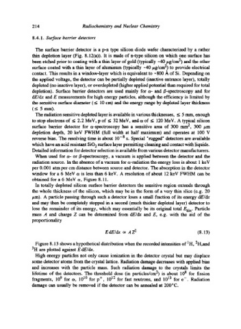
Figure 8.13 shows a hypothetical distribution when the recorded intensities of IH, 2H,and
3H are plotted against E dE/dx.
High energy particles not only cause ionization in the detector crystal but may displace
some detector atoms from the crystal lattice. Radiation damage decreases with applied bias
and increases with the particle mass. Such radiation damage to the crystals limits the
lifetime of the detectors. The threshold dose (in particles/cm 2) is about 108 for fission
fragments, 109 for o~, 1010 for p+, 1012 for fast neutrons, and 1013 for e-. Radiation
damage can usually be removed if the detector can be annealed at 200~