Page 166 - Rashid, Power Electronics Handbook
P. 166

10  Diode Recti®ers                                                                                 155

                                                                            given by

                                                                                    dIðDRÞ       N S      1
                                                                                          ¼ V  IN   ÿ V o          ð10:84Þ
                                                                                      dt         N P     L 1
                                                                            where V is the dc output voltage of the converter.
                                                                                   o
                                                                            The ¯ywheel diode D is reversely biased by Vð9Þ, the
                                                                                              F
                                                                            voltage at node 9
                                                                               Vð9Þ¼ V ðN =N Þ   for  0 < t < DT   ð10:85Þ
                                                                                       IN  S  p
                                                                            The magnetic-reset clamping diode D M  is reversely
                                                                            biased by the negative voltage at node 100. Assuming
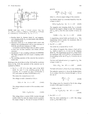
                 FIGURE 10.28  Basic circuit of forward converter. Note that:  that L  and L have the same number of turns, we
                 V IN ¼ 50 V; L 1 ¼ 8 mH; C L ¼ 300 mF; L P ¼ 0:576 mH; L M ¼ 0:576 mH;  M  P
                                                                            have
                 L S ¼ 0:036 mH; R L ¼ 0:35 O; and N P : N M : N S ¼ 4 : 4 : 1.
                                                                                 Vð100Þ¼ ÿV     for  0 < t < DT    ð10:86Þ
                                                                                            IN
                      Recti®er diode D , ¯ywheel diode D , and magnetic-    A magnetizing current builds up linearly in L . This
                                                     F
                                    R
                      reset clamping diode D  are ideal diodes with in®nitely                                      P
                                         M                                  magnetizing current reaches the maximum value of
                      fast switching speed.
                                                                            ðV DTÞ=L at t ¼ DT.
                                                                                     P
                                                                              IN
                      Electronic switch M is an idealized MOS switch with
                                       1
                      in®nitely fast switching speed, with on-state resistance of  2. For DT < t < 2DT
                      0:067 O, and off-state resistance of 1 MO.
                                                                            The switch M is turned off at t ¼ DT.
                                                                                        1
                        It should be noted that PSpice does not allow a switch
                      to have zero on-state resistance and in®nite off-state  The collapse of magnetic ¯ux induces a back emf in
                      resistance.                                           L , which is equal to L , to turn on the clamping
                                                                             M
                                                                                                 P
                      Transformer T has a coupling coef®cient of 0.99999999.  diode D . The magnetizing current in L drops (from
                                                                                                             M
                                                                                   M
                                  1
                      The PSpice program does not accept a coupling coef®-  the maximum value of ðV DTÞ=L , as mentioned in
                                                                                                  IN
                                                                                                         P
                      cient of 1.                                           the preceding) at the rate of V =L . It reaches zero at
                                                                                                     IN
                                                                                                        P
                      The switching operation of the converter has reached a  t ¼ 2DT.
                      steady state.
                                                                            The back emf induced across L is equal to V . The
                                                                                                                  IN
                                                                                                      P
                 Referring to the circuit shown in Fig. 10.28 and the waveforms  voltage at node 3 is
                 shown in Fig. 10.29, the operation of the converter can be
                 explained as follows:                                           Vð3Þ¼ 2V IN  for  DT < t < 2DT    ð10:87Þ
                     1. For 0 < t < DT (D is the duty cycle of the MOS      The back emf across L forces D to stop conducting.
                                                                                                       R
                                                                                              S
                        switch M 1  and T is the switching period of the
                        converter, M 1  is turned on when V1ðVPULSEÞ is     The inductive current in L forces the ¯ywheel diode
                                                                                                  1
                        15 V, and turned off when V1ðVPULSEÞ is 0 V.)       D to conduct. Here IðL Þ (current through L ) falls at
                                                                              F
                                                                                                                 1
                                                                                                1
                                                                            the rate of
                        The switch M is turned on at t ¼ 0.
                                   1
                        The voltage at node 3, denoted as Vð3Þ,is                            dIðL Þ  ¼  ÿV o       ð10:88Þ
                                                                                                1
                                                                                              dt     L
                                                                                                      1
                               Vð3Þ¼ 0  for  0 < t < DT       ð10:82Þ
                                                                            The voltage across D , denoted as Vð6; 9Þ (the voltage
                                                                                             R
                                                                            at node 6 with respect to node 9), is
                        The voltage induced at node 6 of the secondary wind-
                        ing L is                                              VðDRÞ¼ Vð6; 9Þ
                            S
                                                                                    ¼ÿV ðN =N Þ for     DT < t < 2DT
                                                                                         IN
                                                                                             S
                                                                                                P
                                      Vð6Þ¼ V ðN =N Þ         ð10:83Þ                                              ð10:89Þ
                                                    P
                                                 S
                                             IN
                                                                          3. For 2DT < t < T
                        This voltage drives a current I(DR) (current through
                        recti®er diode D ) into the output circuit to produce  Here D M  stops conducting at t ¼ 2DT. The voltage
                                     R
                        the output voltage V . The rate of increase of I(DR) is  across L M  then falls to zero.
                                        o
   161   162   163   164   165   166   167   168   169   170   171